SLUSDT5B September 2019 – October 2023 BQ75614-Q1
PRODUCTION DATA
- 1
- 1 Features
- 2 Applications
- 3 Description
- 4 Revision History
- 5 Description (continued)
- 6 Pin Configuration and Functions
- 7 Specifications
-
8 Detailed Description
- 8.1 Overview
- 8.2 Functional Block Diagram
- 8.3
Feature Description
- 8.3.1 Power Supplies
- 8.3.2 Measurement System
- 8.3.3 Cell Balancing
- 8.3.4 Integrated Hardware Protectors
- 8.3.5 GPIO Configuration
- 8.3.6
Communication, OTP, Diagnostic Control
- 8.3.6.1 Communication
- 8.3.6.2 Fault Handling
- 8.3.6.3 Nonvolatile Memory
- 8.3.6.4 Diagnostic Control/Status
- 8.4 Device Functional Modes
- 8.5
Register Maps
- 8.5.1 OTP Shadow Register Summary
- 8.5.2 Read/Write Register Summary
- 8.5.3 Read-Only Register Summary
- 8.5.4
Register Field Descriptions
- 8.5.4.1 Device Addressing Setup
- 8.5.4.2 Device ID and Scratch Pad
- 8.5.4.3 General Configuration and Control
- 8.5.4.4 Operation Status
- 8.5.4.5 ADC Configuration and Control
- 8.5.4.6
ADC Measurement Results
- 8.5.4.6.1 VCELL16_HI/LO
- 8.5.4.6.2 VCELL15_HI/LO
- 8.5.4.6.3 VCELL14_HI/LO
- 8.5.4.6.4 VCELL13_HI/LO
- 8.5.4.6.5 VCELL12_HI/LO
- 8.5.4.6.6 VCELL11_HI/LO
- 8.5.4.6.7 VCELL10_HI/LO
- 8.5.4.6.8 VCELL9_HI/LO
- 8.5.4.6.9 VCELL8_HI/LO
- 8.5.4.6.10 VCELL7_HI/LO
- 8.5.4.6.11 VCELL6_HI/LO
- 8.5.4.6.12 VCELL5_HI/LO
- 8.5.4.6.13 VCELL4_HI/LO
- 8.5.4.6.14 VCELL3_HI/LO
- 8.5.4.6.15 VCELL2_HI/LO
- 8.5.4.6.16 VCELL1_HI/LO
- 8.5.4.6.17 MAIN_CURRENT_HI/LO
- 8.5.4.6.18 CURRENT_HI/MID/LO
- 8.5.4.6.19 TSREF_HI/LO
- 8.5.4.6.20 GPIO1_HI/LO
- 8.5.4.6.21 GPIO2_HI/LO
- 8.5.4.6.22 GPIO3_HI/LO
- 8.5.4.6.23 GPIO4_HI/LO
- 8.5.4.6.24 GPIO5_HI/LO
- 8.5.4.6.25 GPIO6_HI/LO
- 8.5.4.6.26 GPIO7_HI/LO
- 8.5.4.6.27 GPIO8_HI/LO
- 8.5.4.6.28 DIETEMP1_HI/LO
- 8.5.4.6.29 DIETEMP2_HI/LO
- 8.5.4.6.30 AUX_CELL_HI/LO
- 8.5.4.6.31 AUX_GPIO_HI/LO
- 8.5.4.6.32 AUX_BAT_HI/LO
- 8.5.4.6.33 AUX_REFL_HI/LO
- 8.5.4.6.34 AUX_VBG2_HI/LO
- 8.5.4.6.35 AUX_AVAO_REF_HI/LO
- 8.5.4.6.36 AUX_AVDD_REF_HI/LO
- 8.5.4.6.37 AUX_OV_DAC_HI/LO
- 8.5.4.6.38 AUX_UV_DAC_HI/LO
- 8.5.4.6.39 AUX_OT_OTCB_DAC_HI/LO
- 8.5.4.6.40 AUX_UT_DAC_HI/LO
- 8.5.4.6.41 AUX_VCBDONE_DAC_HI/LO
- 8.5.4.6.42 AUX_VCM_HI/LO
- 8.5.4.6.43 REFOVDAC_HI/LO
- 8.5.4.6.44 DIAG_MAIN_HI/LO
- 8.5.4.6.45 DIAG_AUX_HI/LO
- 8.5.4.7 Balancing Configuration, Control and Status
- 8.5.4.8 Protector Configuration and Control
- 8.5.4.9 GPIO Configuration
- 8.5.4.10 SPI Master
- 8.5.4.11 Diagnostic Control
- 8.5.4.12 Fault Configuration and Reset
- 8.5.4.13
Fault Status
- 8.5.4.13.1 FAULT_SUMMARY
- 8.5.4.13.2 FAULT_COMM1
- 8.5.4.13.3 FAULT_OTP
- 8.5.4.13.4 FAULT_SYS
- 8.5.4.13.5 FAULT_PROT1
- 8.5.4.13.6 FAULT_PROT2
- 8.5.4.13.7 FAULT_OV1
- 8.5.4.13.8 FAULT_OV2
- 8.5.4.13.9 FAULT_UV1
- 8.5.4.13.10 FAULT_UV2
- 8.5.4.13.11 FAULT_OT
- 8.5.4.13.12 FAULT_UT
- 8.5.4.13.13 FAULT_COMP_GPIO
- 8.5.4.13.14 FAULT_COMP_VCCB1
- 8.5.4.13.15 FAULT_COMP_VCCB2
- 8.5.4.13.16 FAULT_COMP_VCOW1
- 8.5.4.13.17 FAULT_COMP_VCOW2
- 8.5.4.13.18 FAULT_COMP_CBOW1
- 8.5.4.13.19 FAULT_COMP_CBOW2
- 8.5.4.13.20 FAULT_COMP_CBFET1
- 8.5.4.13.21 FAULT_COMP_CBFET2
- 8.5.4.13.22 FAULT_COMP_MISC
- 8.5.4.13.23 FAULT_PWR1
- 8.5.4.13.24 FAULT_PWR2
- 8.5.4.13.25 FAULT_PWR3
- 8.5.4.14 Debug Control and Status
- 8.5.4.15
OTP Programming Control and Status
- 8.5.4.15.1 OTP_PROG_UNLOCK1A through OTP_PROG_UNLOCK1D
- 8.5.4.15.2 OTP_PROG_UNLOCK2A through OTP_PROG_UNLOCK2D
- 8.5.4.15.3 OTP_PROG_CTRL
- 8.5.4.15.4 OTP_ECC_TEST
- 8.5.4.15.5 OTP_ECC_DATAIN1 through OTP_ECC_DATAIN9
- 8.5.4.15.6 OTP_ECC_DATAOUT1 through OTP_ECC_DATAOUT9
- 8.5.4.15.7 OTP_PROG_STAT
- 8.5.4.15.8 OTP_CUST1_STAT
- 8.5.4.15.9 OTP_CUST2_STAT
- 9 Application and Implementation
- 10Power Supply Recommendations
- 11Layout
- 12Device and Documentation Support
- 13Mechanical, Packaging, and Orderable Information
Package Options
Mechanical Data (Package|Pins)
- PAP|64
Thermal pad, mechanical data (Package|Pins)
- PAP|64
Orderable Information
8.4 Device Functional Modes
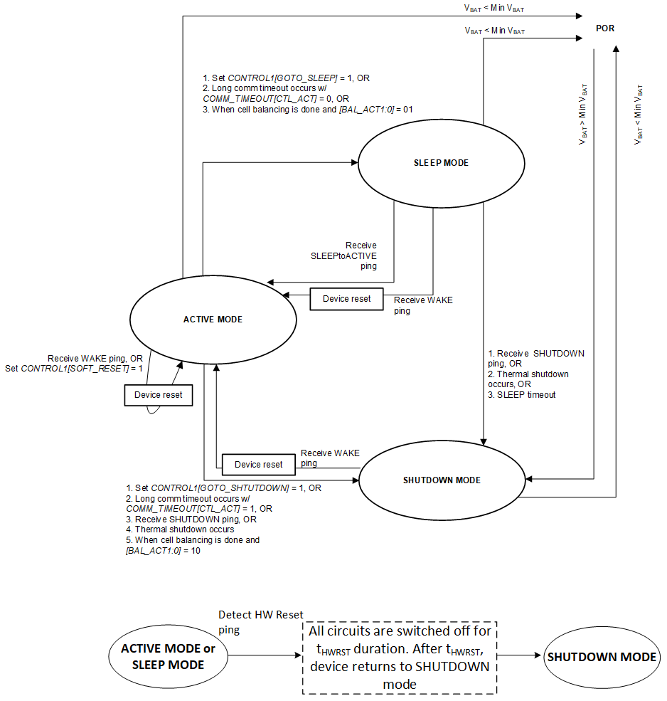
The device has three power modes plus an POR state.
- POR: This is not a power mode. This is a condition in which the voltage at the BAT pin is less than VBAT min, and all circuits including the AVAO_REF block in the device are powered off.
- SHUTDOWN: This is the lowest power mode. AVDD, DVDD and CVDD supplies are off. Only a gross regulation at LDOIN pin is maintained. CVDD pin is will have a similar voltage as the LDOIN pin through internal circuit in order to support WAKE detection.
- SLEEP: This is the low power operation mode. Only limited functions are available.
- ACTIVE: This is the full power operation mode. All functions are supported under this state.
The various functions supported under different power modes are summarized in Table 8-26 and the power state diagram is shown in Figure 8-36.
Table 8-26 Active Functions Summary
| Functional Block | SHUTDOWN | SLEEP | ACTIVE | POR |
|---|---|---|---|---|
| Main ADC and CS ADC | √ | This is not a power state. All circuits are off. A sufficient voltage on VBAT will POR the device and put it to SHUTDOWN mode | ||
| AUX ADC | √ | |||
| OV/UV protector | √(1) | √ | ||
| OT/UT protector | √(1) | √ | ||
| Cell Balancing | √(1) | √ | ||
| OTCB Detection | √(1) | √ | ||
| UART | √ | |||
| Comm Vertical Communication | √ | |||
| Fault Status and NFAULT Communication | √ | √ | ||
| Comm timeout | √ | |||
| SLEEP timeout | √ | |||
| Thermal Shutdown Detection | √ | √ | ||
| SPI Master | √ | |||
| OTP programming | √ | |||
| Always-on block to detect POR of the device | √ | √ | √ |
(1) To enable cell balancing, OV/UV or OT/UT protector(s) in SLEEP mode, host must
enable the function(s) in ACTIVE mode first, then put the device to SLEEP.
 Figure 8-36 Power State Diagram