SLUSE96 November 2023 BQ76907
PRODUCTION DATA
- 1
- 1 Features
- 2 Applications
- 3 Description
- 4 Device Comparison Table
- 5 Pin Configuration and Functions
-
6 Specifications
- 6.1 Absolute Maximum Ratings
- 6.2 ESD Ratings
- 6.3 Recommended Operating Conditions
- 6.4 Thermal Information bq76907
- 6.5 Supply Current
- 6.6 Digital I/O
- 6.7 REGOUT LDO
- 6.8 Voltage References
- 6.9 Coulomb Counter
- 6.10 Coulomb Counter Digital Filter
- 6.11 Current Wake Detector
- 6.12 Analog-to-Digital Converter
- 6.13 Cell Balancing
- 6.14 Internal Temperature Sensor
- 6.15 Thermistor Measurement
- 6.16 Hardware Overtemperature Detector
- 6.17 Internal Oscillator
- 6.18 Charge and Discharge FET Drivers
- 6.19 Comparator-Based Protection Subsystem
- 6.20 Timing Requirements - I2C Interface, 100kHz Mode
- 6.21 Timing Requirements - I2C Interface, 400kHz Mode
- 6.22 Timing Diagram
- 6.23 Typical Characteristics
- 7 Detailed Description
- 8 Application and Implementation
- 9 Power Supply Recommendations
- 10Layout
- 11Device and Documentation Support
- 12Revision History
- 13Introduction to Mechanical, Packaging, and Orderable Information
Package Options
Mechanical Data (Package|Pins)
- RGR|20
Thermal pad, mechanical data (Package|Pins)
- RGR|20
Orderable Information
7.4.10 I2C Serial Communications Interface
The I2C serial communications interface in the BQ76907 acts as a target device and supports rates up to 400 kHz with an optional CRC check. The BQ76907 will initially power up by default in a mode determined by the OTP settings factory programmed by TI. The host can change the CRC mode setting while in CONFIG_UPDATE mode, then the new setting will take effect upon exit of CONFIG_UPDATE mode.
The I2C device address (as an 8-bit value including target address and R/W bit) is set by default as 0x10 (write), 0x11 (read), which can also be changed by the configuration setting.
The communications interface includes programmable timeout capability, with the internal I2C bus logic reset when an enabled timeout occurs. This is described in detail in the BQ76907 Technical Reference Manual.
An I2C write transaction is shown in Figure 7-1. Block writes are allowed by sending additional data bytes before the Stop. The I2C logic will auto-increment the register address after each data byte. The shaded regions show when the device may be clock stretching.

Figure 7-1 I2C Write
The CRC check is enabled by setting a data memory bit. When enabled, the CRC is calculated as follows:
- Note that the CRC is reset after each data byte and after each stop.
- In a single-byte write transaction, the CRC is calculated over the target address, register address, and data.
- In a block write transaction, the CRC for the first data byte is calculated over the target address, register address, and data. The CRC for subsequent data bytes is calculated over the data byte only.
The CRC polynomial is x8 + x2 + x + 1, and the initial value is 0.
When the target detects an invalid CRC, the I2C target will NACK the CRC, which causes the I2C target to go to an idle state.
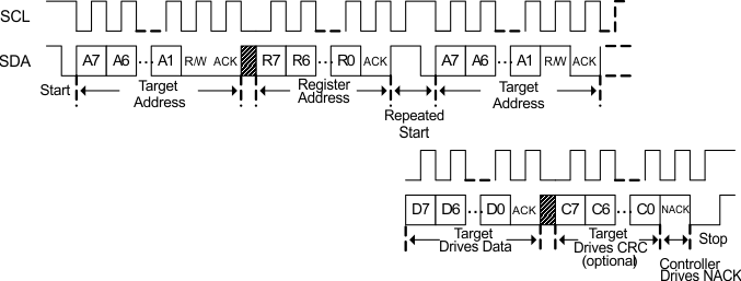
Figure 7-2 shows a read transaction using a Repeated Start. The shaded regions show when the device may be clock stretching.

Figure 7-2 I2C Read with Repeated Start
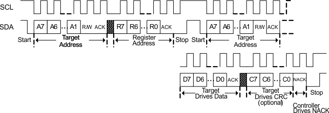
Figure 7-3 shows a read transaction where a Repeated Start is not used, for example if not available in hardware. For a block read, the controller ACK’s each data byte except the last and continues to clock the interface. The I2C block will auto-increment the register address after each data byte. The shaded regions show when the device may be clock stretching.

Figure 7-3 I2C Read Without Repeated Start
When enabled, the CRC for a read transaction is calculated as follows:
- Note that the CRC is reset after each data byte and after each stop.
- In a single-byte read transaction using a repeated start, the CRC is calculated beginning at the first start, so will include the target address, the register address, then the target address with read bit set, then the data byte.
- In a single-byte read transaction using a stop after the initial register address, the CRC is reset after the stop, so will only include the target address with read bit set and the data byte.
- In a block read transaction using repeated starts, the CRC for the first data byte is calculated beginning at the first start and will include the target address, the register address, then the target address with read bit set, then the data byte. The CRC for subsequent data bytes is calculated over the data byte only.
- In a block read transaction using a stop after the initial register address, the CRC is reset after the stop, so will only include the target address with read bit set and the first data byte. The CRC for subsequent data bytes is calculated over the data byte only.
The CRC polynomial is x8 + x2 + x + 1, and the initial value is 0.
When the controller detects an invalid CRC, the I2C controller will NACK the CRC, which causes the I2C target to go to an idle state.
For more information, see the BQ76907 Technical Reference Manual.