SLUSE96 November 2023 BQ76907
PRODUCTION DATA
- 1
- 1 Features
- 2 Applications
- 3 Description
- 4 Device Comparison Table
- 5 Pin Configuration and Functions
-
6 Specifications
- 6.1 Absolute Maximum Ratings
- 6.2 ESD Ratings
- 6.3 Recommended Operating Conditions
- 6.4 Thermal Information bq76907
- 6.5 Supply Current
- 6.6 Digital I/O
- 6.7 REGOUT LDO
- 6.8 Voltage References
- 6.9 Coulomb Counter
- 6.10 Coulomb Counter Digital Filter
- 6.11 Current Wake Detector
- 6.12 Analog-to-Digital Converter
- 6.13 Cell Balancing
- 6.14 Internal Temperature Sensor
- 6.15 Thermistor Measurement
- 6.16 Hardware Overtemperature Detector
- 6.17 Internal Oscillator
- 6.18 Charge and Discharge FET Drivers
- 6.19 Comparator-Based Protection Subsystem
- 6.20 Timing Requirements - I2C Interface, 100kHz Mode
- 6.21 Timing Requirements - I2C Interface, 400kHz Mode
- 6.22 Timing Diagram
- 6.23 Typical Characteristics
- 7 Detailed Description
- 8 Application and Implementation
- 9 Power Supply Recommendations
- 10Layout
- 11Device and Documentation Support
- 12Revision History
- 13Introduction to Mechanical, Packaging, and Orderable Information
Package Options
Mechanical Data (Package|Pins)
- RGR|20
Thermal pad, mechanical data (Package|Pins)
- RGR|20
Orderable Information
5 Pin Configuration and Functions
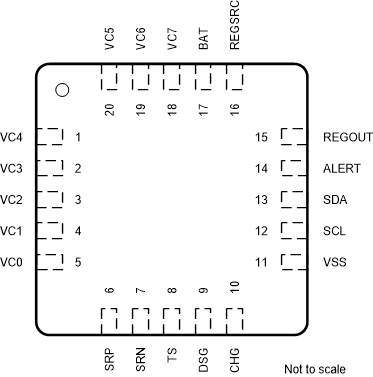
 Figure 5-1 BQ76907 Pinout
Table 5-1 Pin
Functions
| PIN | I/O | TYPE | DESCRIPTION | |
|---|---|---|---|---|
| NO. | NAME | |||
| 1 | VC4 | I | IA | Sense voltage input pin for the fourth cell from the bottom of the stack, balance current input for the fourth cell from the bottom of the stack, and return balance current for the fifth cell from the bottom of the stack |
| 2 | VC3 | I | IA | Sense voltage input pin for third cell from the bottom of the stack, balance current input for third cell from the bottom of the stack, and return balance current for the fourth cell from the bottom of the stack |
| 3 | VC2 | I | IA | Sense voltage input pin for second cell from the bottom of the stack, balance current input for second cell from the bottom of the stack, and return balance current for third cell from the bottom of the stack |
| 4 | VC1 | I | IA | Sense voltage input pin for first cell from the bottom of the stack, balance current input for first cell from the bottom of the stack, and return balance current for second cell from the bottom of the stack |
| 5 | VC0 | I | IA | Sense voltage input pin for negative terminal of the first cell from the bottom of the stack, and return balance current for first cell from the bottom of the stack |
| 6 | SRP | I | IA | Analog input pin connected to the internal coulomb counter peripheral for integrating a small voltage between SRP and SRN, where SRP is the top of the sense resistor. A charging current generates a positive voltage at SRP relative to SRN. |
| 7 | SRN | I | IA | Analog input pin connected to the internal coulomb counter peripheral for integrating a small voltage between SRP and SRN, where SRN is the bottom of the sense resistor. A charging current generates a positive voltage at SRP relative to SRN. |
| 8 | TS | I/O | I/OA | Thermistor or general-purpose ADC input and functions as a wakeup from SHUTDOWN, |
| 9 | DSG | O | OA | NMOS Discharge FET drive output pin |
| 10 | CHG | O | OA | NMOS Charge FET drive output pin |
| 11 | VSS | — | P | Device ground |
| 12 | SCL | I/O | I/OD | I2C serial communication bus clock |
| 13 | SDA | I/O | I/OD | I2C serial communication bus data |
| 14 | ALERT | O | OD | Digital interrupt output pin |
| 15 | REGOUT | O | OA | LDO output, which can be programmed for 1.8 V, 2.5 V, 3.0 V,3.3 V, or 5.0 V. |
| 16 | REGSRC | I | IA | Input pin for REGOUT LDO, also functions as supply for the CHG and DSG FET drivers. |
| 17 | BAT | I | P | Primary power supply input pin |
| 18 | VC7 | I | IA | Sense voltage input pin for the seventh cell from the bottom of the stack, balance current input for the seventh cell from the bottom of the stack, and top-of-stack measurement point |
| 19 | VC6 | I | IA | Sense voltage input pin for the sixth cell from the bottom of the stack, balance current input for the sixth cell from the bottom of the stack, and return balance current for the seventh cell from the bottom of the stack |
| 20 | VC5 | I | IA | Sense voltage input pin for the fifth cell from the bottom of the stack, balance current input for the fifth cell from the bottom of the stack, and return balance current for the sixth cell from the bottom of the stack |