SLUSE96 November 2023 BQ76907
PRODUCTION DATA
- 1
- 1 Features
- 2 Applications
- 3 Description
- 4 Device Comparison Table
- 5 Pin Configuration and Functions
-
6 Specifications
- 6.1 Absolute Maximum Ratings
- 6.2 ESD Ratings
- 6.3 Recommended Operating Conditions
- 6.4 Thermal Information bq76907
- 6.5 Supply Current
- 6.6 Digital I/O
- 6.7 REGOUT LDO
- 6.8 Voltage References
- 6.9 Coulomb Counter
- 6.10 Coulomb Counter Digital Filter
- 6.11 Current Wake Detector
- 6.12 Analog-to-Digital Converter
- 6.13 Cell Balancing
- 6.14 Internal Temperature Sensor
- 6.15 Thermistor Measurement
- 6.16 Hardware Overtemperature Detector
- 6.17 Internal Oscillator
- 6.18 Charge and Discharge FET Drivers
- 6.19 Comparator-Based Protection Subsystem
- 6.20 Timing Requirements - I2C Interface, 100kHz Mode
- 6.21 Timing Requirements - I2C Interface, 400kHz Mode
- 6.22 Timing Diagram
- 6.23 Typical Characteristics
- 7 Detailed Description
- 8 Application and Implementation
- 9 Power Supply Recommendations
- 10Layout
- 11Device and Documentation Support
- 12Revision History
- 13Introduction to Mechanical, Packaging, and Orderable Information
Package Options
Mechanical Data (Package|Pins)
- RGR|20
Thermal pad, mechanical data (Package|Pins)
- RGR|20
Orderable Information
8.2.3 Application Performance Plot
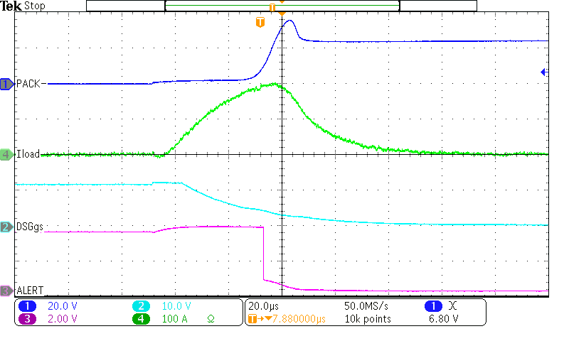
The scope plot below shows the response of the device to a short circuit in discharge (SCD) event and subsequent protection. The device was configured with SCD threshold = 10 mV and SCD delay of 0 ~ 15 μs. A short circuit was applied through a 1 mΩ sense resistor. The input filter network on the SRP and SRN pins consisted of 100 Ω resistors and a 100 nF differential capacitor, which results in a 20 μs time constant. The [SSA] bit in Alarm Status() causes the ALERT pin to fall, which occurs between approximately 15 μs and 30 μs after the safety status is triggered and the DSG driver is disabled. The circuit included a 5.1 kΩ resistor between the DSG pin and the DSG FET gate.
 Figure 8-4 Scope plot of SCD event and
protection. Load current measured directly at the SRN-SRP pins, which includes
an RC delay versus the voltage at the sense resistor.