SLUSE91B September 2020 – January 2022 BQ769142
PRODUCTION DATA
- 1 Features
- 2 Applications
- 3 Description
- 4 Revision History
- 5 Device Comparison Table
- 6 Pin Configuration and Functions
-
7 Specifications
- 7.1 Absolute Maximum Ratings
- 7.2 ESD Ratings
- 7.3 Recommended Operating Conditions
- 7.4 Thermal Information BQ769142
- 7.5 Supply Current
- 7.6 Digital I/O
- 7.7 LD Pin
- 7.8 Precharge (PCHG) and Predischarge (PDSG) FET Drive
- 7.9 FUSE Pin Functionality
- 7.10 REG18 LDO
- 7.11 REG0 Pre-regulator
- 7.12 REG1 LDO
- 7.13 REG2 LDO
- 7.14 Voltage References
- 7.15 Coulomb Counter
- 7.16 Coulomb Counter Digital Filter (CC1)
- 7.17 Current Measurement Digital Filter (CC2)
- 7.18 Current Wake Detector
- 7.19 Analog-to-Digital Converter
- 7.20 Cell Balancing
- 7.21 Cell Open Wire Detector
- 7.22 Internal Temperature Sensor
- 7.23 Thermistor Measurement
- 7.24 Internal Oscillators
- 7.25 High-side NFET Drivers
- 7.26 Comparator-Based Protection Subsystem
- 7.27 Timing Requirements - I2C Interface, 100kHz Mode
- 7.28 Timing Requirements - I2C Interface, 400kHz Mode
- 7.29 Timing Requirements - HDQ Interface
- 7.30 Timing Requirements - SPI Interface
- 7.31 Interface Timing Diagrams
- 7.32 Typical Characteristics
- 8 Device Description
- 9 Device Configuration
-
10Measurement Subsystem
- 10.1 Voltage Measurement
- 10.2 General Purpose ADCIN Functionality
- 10.3 Coulomb Counter and Digital Filters
- 10.4 Synchronized Voltage and Current Measurement
- 10.5 Internal Temperature Measurement
- 10.6 Thermistor Temperature Measurement
- 10.7 Factory Trim of Voltage ADC
- 10.8 Voltage Calibration (ADC Measurements)
- 10.9 Voltage Calibration (COV and CUV Protections)
- 10.10 Current Calibration
- 10.11 Temperature Calibration
- 11Primary and Secondary Protection Subsystems
-
12Device
Hardware Features
- 12.1 Voltage References
- 12.2 ADC Multiplexer
- 12.3 LDOs
- 12.4 Standalone Versus Host Interface
- 12.5 Multifunction Pin Controls
- 12.6 RST_SHUT Pin Operation
- 12.7 CFETOFF, DFETOFF, and BOTHOFF Pin Functionality
- 12.8 ALERT Pin Operation
- 12.9 DDSG and DCHG Pin Operation
- 12.10 Fuse Drive
- 12.11 Cell Open Wire
- 12.12 Low Frequency Oscillator
- 12.13 High Frequency Oscillator
- 13Device Functional Modes
- 14Serial Communications Interface
- 15Cell Balancing
- 16Application and Implementation
- 17Power Supply Requirements
- 18Layout
- 19Device and Documentation Support
- 20Mechanical, Packaging, Orderable Information
Package Options
Mechanical Data (Package|Pins)
- PFB|48
Thermal pad, mechanical data (Package|Pins)
Orderable Information
13.1 Overview
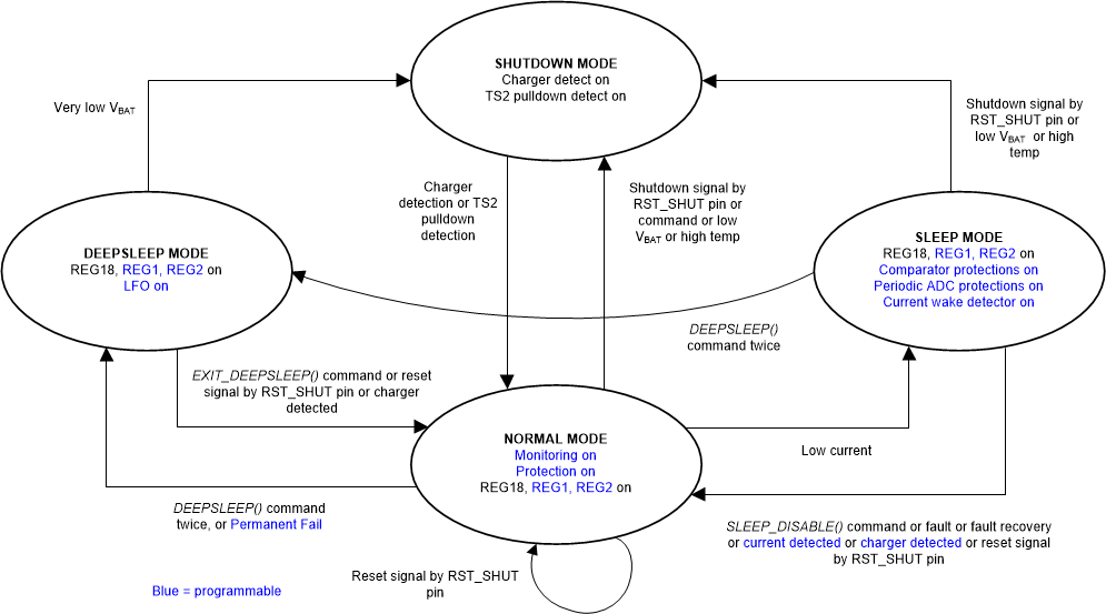
This device supports four functional modes to support optimized features and power dissipation, with the device able to transition between modes either autonomously or controlled by a host processor.
- NORMAL mode: In this mode, the device performs frequent measurements of system current, cell voltages, internal and thermistor temperature, and various other voltages, operates protections as configured, and provides data and status updates.
- SLEEP mode: In this mode, the DSG FET is enabled, the CHG FET can optionally be disabled, and the device performs measurements, calculations, and data updates in adjustable time intervals. Battery protections are still enabled. Between the measurement intervals, the device is operating in a reduced power stage to minimize total average current consumption.
- DEEPSLEEP mode: In this mode, the CHG, PCHG, DSG, and PDSG FETs are disabled, all battery protections are disabled, and no current or voltage measurements are taken. The REG1 and REG2 LDOs can be kept powered, in order to maintain power to external circuitry, such as a host processor.
- SHUTDOWN mode: The device is completely disabled (including the internal, REG1, and REG2 LDOs), the CHG, PCHG, DSG, and PDSG FETs are all disabled, all battery protections are disabled, and no measurements are taken. This is the lowest power state of the device, which may be used for shipment or long-term storage. All register settings are lost when in SHUTDOWN mode.
The device also includes a CONFIG_UPDATE mode, which is used for parameter updates. Figure 13-1 shows the transitions between the functional modes.
 Figure 13-1 Device
Functional Modes