SLUSE14B December 2020 – December 2021 BQ76942
PRODUCTION DATA
- 1 Features
- 2 Applications
- 3 Description
- 4 Revision History
- 5 Device Comparison Table
- 6 Pin Configuration and Functions
-
7 Specifications
- 7.1 Absolute Maximum Ratings
- 7.2 ESD Ratings
- 7.3 Recommended Operating Conditions
- 7.4 Thermal Information BQ76942
- 7.5 Supply Current
- 7.6 Digital I/O
- 7.7 LD Pin
- 7.8 Precharge (PCHG) and Predischarge (PDSG) FET Drive
- 7.9 FUSE Pin Functionality
- 7.10 REG18 LDO
- 7.11 REG0 Pre-regulator
- 7.12 REG1 LDO
- 7.13 REG2 LDO
- 7.14 Voltage References
- 7.15 Coulomb Counter
- 7.16 Coulomb Counter Digital Filter (CC1)
- 7.17 Current Measurement Digital Filter (CC2)
- 7.18 Current Wake Detector
- 7.19 Analog-to-Digital Converter
- 7.20 Cell Balancing
- 7.21 Cell Open Wire Detector
- 7.22 Internal Temperature Sensor
- 7.23 Thermistor Measurement
- 7.24 Internal Oscillators
- 7.25 High-Side NFET Drivers
- 7.26 Comparator-Based Protection Subsystem
- 7.27 Timing Requirements – I2C Interface, 100kHz Mode
- 7.28 Timing Requirements – I2C Interface, 400kHz Mode
- 7.29 Timing Requirements – HDQ Interface
- 7.30 Timing Requirements – SPI Interface
- 7.31 Interface Timing Diagrams
- 7.32 Typical Characteristics
- 8 Device Description
- 9 Device Configuration
-
10Measurement Subsystem
- 10.1 Voltage Measurement
- 10.2 General Purpose ADCIN Functionality
- 10.3 Coulomb Counter and Digital Filters
- 10.4 Synchronized Voltage and Current Measurement
- 10.5 Internal Temperature Measurement
- 10.6 Thermistor Temperature Measurement
- 10.7 Factory Trim of Voltage ADC
- 10.8 Voltage Calibration (ADC Measurements)
- 10.9 Voltage Calibration (COV and CUV Protections)
- 10.10 Current Calibration
- 10.11 Temperature Calibration
- 11Primary and Secondary Protection Subsystems
-
12Device Hardware Features
- 12.1 Voltage References
- 12.2 ADC Multiplexer
- 12.3 LDOs
- 12.4 Standalone Versus Host Interface
- 12.5 Multifunction Pin Controls
- 12.6 RST_SHUT Pin Operation
- 12.7 CFETOFF, DFETOFF, BOTHOFF Pin Functionality
- 12.8 ALERT Pin Operation
- 12.9 DDSG and DCHG Pin Operation
- 12.10 Fuse Drive
- 12.11 Cell Open Wire
- 12.12 Low Frequency Oscillator
- 12.13 High Frequency Oscillator
- 13Device Functional Modes
- 14Serial Communications Interface
- 15Cell Balancing
- 16Application and Implementation
- 17Power Supply Requirements
- 18Layout
- 19Device and Documentation Support
- 20Mechanical, Packaging, Orderable Information
Package Options
Mechanical Data (Package|Pins)
- PFB|48
Thermal pad, mechanical data (Package|Pins)
Orderable Information
10.1.2 Usage of VC Pins for Cells Versus Interconnect
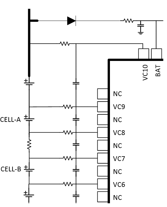
If the BQ76942 device is used in a system with fewer than 10-series cells, the additional cell inputs can be used to improve measurement performance. For example, a long connection may exist between two cells in a pack, such that there may be significant interconnect resistance between the cells, such as shown in Figure 10-1 between CELL-A and CELL-B. By connecting VC7 close to the positive terminal of CELL-B, and connecting VC8 close to the negative terminal of CELL-A, more accurate cell voltage measurements are obtained for CELL-A and CELL-B, since the I·R voltage across the interconnect resistance between the cells is not included in either cell voltage measurement. Because the device reports the voltage across the interconnect resistance and the synchronized current, the resistance of the interconnect between CELL-A and CELL-B can also be calculated and monitored during operation. It is recommended to include the series resistance and bypass capacitor on cell inputs connected in this manner, as shown below.
 Figure 10-1 Using Cell Input Pins for Interconnect
Measurement
Figure 10-1 Using Cell Input Pins for Interconnect
MeasurementIf this connection across an interconnect is not needed (or it is preferred to avoid the extra resistor and capacitor), then unused cell input pins should be shorted to adjacent cell input pins, as shown in Figure 10-2 for VC8.
 Figure 10-2 Terminating an Unused Cell Input
Pin
Figure 10-2 Terminating an Unused Cell Input
PinA configuration register is used to specify which cell inputs are used for actual cells. The device uses this information to disable cell voltage protections associated with inputs that are used to measure interconnect or are not used at all. Voltage measurements for all inputs are reported in a 16-bit format (in units of mV), as well as 32-bit format (in units of raw ADC counts), irrespective of whether they are used for cells or not.