SLUSE13B January 2020 – November 2021 BQ76952
PRODUCTION DATA
- 1 Features
- 2 Applications
- 3 Description
- 4 Revision History
- 5 Device Comparison Table
- 6 Pin Configuration and Functions
-
7 Specifications
- 7.1 Absolute Maximum Ratings
- 7.2 ESD Ratings
- 7.3 Recommended Operating Conditions
- 7.4 Thermal Information BQ76952
- 7.5 Supply Current
- 7.6 Digital I/O
- 7.7 LD Pin
- 7.8 Precharge (PCHG) and Predischarge (PDSG) FET Drive
- 7.9 FUSE Pin Functionality
- 7.10 REG18 LDO
- 7.11 REG0 Pre-regulator
- 7.12 REG1 LDO
- 7.13 REG2 LDO
- 7.14 Voltage References
- 7.15 Coulomb Counter
- 7.16 Coulomb Counter Digital Filter (CC1)
- 7.17 Current Measurement Digital Filter (CC2)
- 7.18 Current Wake Detector
- 7.19 Analog-to-Digital Converter
- 7.20 Cell Balancing
- 7.21 Cell Open Wire Detector
- 7.22 Internal Temperature Sensor
- 7.23 Thermistor Measurement
- 7.24 Internal Oscillators
- 7.25 High-side NFET Drivers
- 7.26 Comparator-Based Protection Subsystem
- 7.27 Timing Requirements - I2C Interface, 100kHz Mode
- 7.28 Timing Requirements - I2C Interface, 400kHz Mode
- 7.29 Timing Requirements - HDQ Interface
- 7.30 Timing Requirements - SPI Interface
- 7.31 Interface Timing Diagrams
- 7.32 Typical Characteristics
- 8 Device Description
- 9 Device Configuration
-
10Measurement Subsystem
- 10.1 Voltage Measurement
- 10.2 General Purpose ADCIN Functionality
- 10.3 Coulomb Counter and Digital Filters
- 10.4 Synchronized Voltage and Current Measurement
- 10.5 Internal Temperature Measurement
- 10.6 Thermistor Temperature Measurement
- 10.7 Factory Trim of Voltage ADC
- 10.8 Voltage Calibration (ADC Measurements)
- 10.9 Voltage Calibration (COV and CUV Protections)
- 10.10 Current Calibration
- 10.11 Temperature Calibration
- 11Primary and Secondary Protection Subsystems
-
12Device
Hardware Features
- 12.1 Voltage References
- 12.2 ADC Multiplexer
- 12.3 LDOs
- 12.4 Standalone Versus Host Interface
- 12.5 Multifunction Pin Controls
- 12.6 RST_SHUT Pin Operation
- 12.7 CFETOFF, DFETOFF, and BOTHOFF Pin Functionality
- 12.8 ALERT Pin Operation
- 12.9 DDSG and DCHG Pin Operation
- 12.10 Fuse Drive
- 12.11 Cell Open Wire
- 12.12 Low Frequency Oscillator
- 12.13 High Frequency Oscillator
- 13Device Functional Modes
- 14Serial Communications Interface
- 15Cell Balancing
- 16Application and Implementation
- 17Power Supply Requirements
- 18Layout
- 19Device and Documentation Support
- 20Mechanical, Packaging, Orderable Information
Package Options
Mechanical Data (Package|Pins)
- PFB|48
Thermal pad, mechanical data (Package|Pins)
Orderable Information
16.5 FET Driver Turn-Off
The high-side CHG and DSG FET drivers operate differently when they are triggered to turn off their respective FET. The CHG driver includes an internal switch which discharges the CHG pin toward the BAT pin level. The DSG FET driver will discharge the DSG pin toward the LD pin level, but it includes a more complex structure than just a switch, to support a faster turn off.
When the DSG driver is triggered to turn off, the device will initially begin discharging the DSG pin toward VSS. However, since the PACK+ terminal may not fall to a voltage near VSS quickly, the DSG FET gate should not be driven significantly below PACK+, otherwise the DSG FET may be damaged due to excessive negative gate-source voltage. Thus, the device monitors the voltage on the LD pin (which is connected to PACK+ through an external series resistor) and will stop the discharge when the DSG pin voltage drops below the LD pin voltage. When the discharge has stopped, the DSG pin voltage may relax back above the LD pin voltage, at which point the device will again discharge the DSG pin toward VSS, until the DSG gate voltage again falls below the LD pin voltage. This repeats in a series of pulses which over time discharge the DSG gate to the voltage of the LD pin. This pulsing continues for approximately 100 to 200 μs, after which the driver remains in a high impedance state if within approximately 500 mV of the voltage of the LD pin. The external resistor between the DSG gate and source then discharges the remaining FET VGS voltage so the FET remains off.
The external series gate resistor between the DSG pin and the DSG FET gate is used to adjust the speed of the turn-off transient. A low resistance (such as 100 Ω) will provide a fast turn-off during a short circuit event, but this may result in an overly large inductive spike at the top of stack when the FET is disabled. A larger resistor value (such as 1 kΩ or 4.7 kΩ) will reduce this speed and the corresponding inductive spike level.
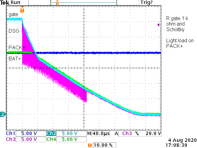
Oscilloscope captures of DSG driver turn-off are shown below, with the DSG pin driving the gate of a CSD19536KCS NFET, which has a typical Ciss of 9250 pF. Figure 16-6 shows the signals when using a 1-kΩ series gate resistor between the DSG pin and the FET gate, and a light load on PACK+, such that the voltage on PACK+ drops slowly as the FET is disabled. The pulsing on the DSG pin can be seen lasting for approximately 170 μs.

Figure 16-6 Moderate Speed DSG FET Turn-Off, Using a 1-kΩ Series Gate Resistor, and a Light Load on PACK+.
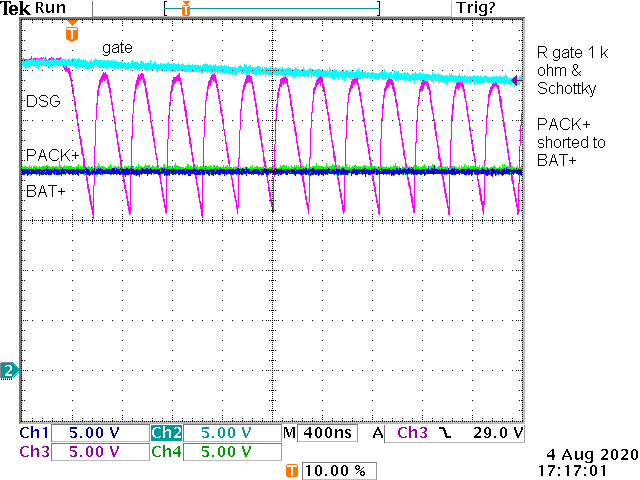
A zoomed-in version of the pulsing generated by the DSG pin is shown in Figure 16-7, this time with PACK+ shorted to the top of stack.

Figure 16-7 Zoomed-In View of the Pulsing on the DSG Pin During FET Turn-Off
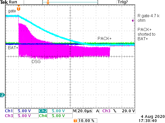
A slower turn-off case is shown in Figure 16-8, using a 4.7-kΩ series gate resistor, and the PACK+ connector shorted to the top of stack.

Figure 16-8 A Slower Turn-Off Case Using a 4.7-kΩ Series Gate Resistor, and the PACK+ Connector Shorted to the Top of the Stack
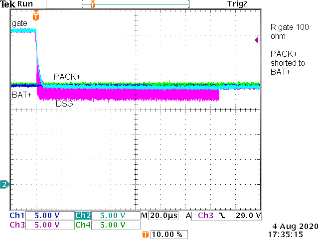
A fast turn-off case is shown in Figure 16-9, in which a 100-Ω series gate resistor is used between the DSG pin and the FET gate.

Figure 16-9 A Fast Turn-Off Case with a 100-Ω Series Gate Resistor