SLUSE36J July 2021 – November 2023 BQ77216
PRODUCTION DATA
- 1
- 1 Features
- 2 Applications
- 3 Description
- 4 Description (continued)
- 5 Device Comparison Table
- 6 Pin Configuration and Functions
- 7 Specifications
- 8 Detailed Description
- 9 Application and Implementation
- 10Power Supply Recommendations
- 11Layout
- 12Device and Documentation Support
- 13Revision History
- 14Mechanical, Packaging, and Orderable Information
Package Options
Mechanical Data (Package|Pins)
- PW|24
Thermal pad, mechanical data (Package|Pins)
Orderable Information
8.3.1 Voltage Fault Detection
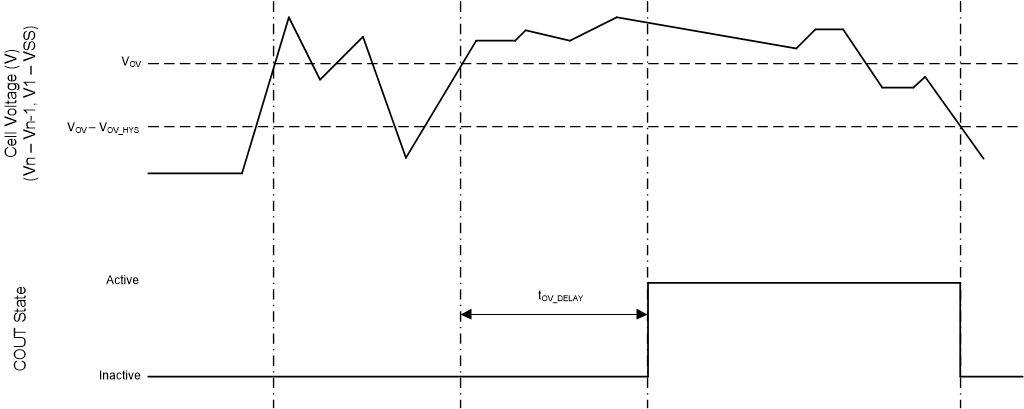
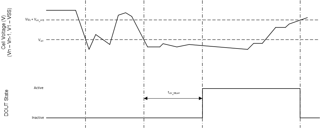
In the BQ77216 device, each cell is monitored independently. Overvoltage is detected by comparing the actual cell voltage to a protection voltage reference, VOV. If any cell voltage exceeds the programmed OV value, a timer circuit is activated. When the timer expires, the COUT pin goes from inactive to active state. The timer is reset if the cell voltage falls below the recovery threshold (VOV – VOV_HYS). Undervoltage is detected by comparing the actual cell voltage to a protection voltage reference, VUV. If any cell voltage falls below the programmed UV value, a timer circuit is activated. When the timer expires, the DOUT pin goes from inactive to active state. The timer is reset if the cell voltage rises below the recovery threshold (VUV + VUV_HYS).
 Figure 8-1 Timing for Overvoltage Sensing
 Figure 8-2 Timing for Undervoltage Sensing