SLUSF60 December 2023 BQ77307
PRODUCTION DATA
- 1
- 1 Features
- 2 Applications
- 3 Description
- 4 Device Comparison Table
- 5 Pin Configuration and Functions
-
6 Specifications
- 6.1 Absolute Maximum Ratings
- 6.2 ESD Ratings
- 6.3 Recommended Operating Conditions
- 6.4 Thermal Information BQ77307
- 6.5 Supply Current
- 6.6 Digital I/O
- 6.7 REGOUT LDO
- 6.8 Voltage References
- 6.9 Current Detector
- 6.10 Thermistor Pullup Resistor
- 6.11 Hardware Overtemperature Detector
- 6.12 Internal Oscillator
- 6.13 Charge and Discharge FET Drivers
- 6.14 Protection Subsystem
- 6.15 Timing Requirements - I2C Interface, 100kHz Mode
- 6.16 Timing Requirements - I2C Interface, 400kHz Mode
- 6.17 Timing Diagram
- 6.18 Typical Characteristics
-
7 Detailed Description
- 7.1 Overview
- 7.2 Functional Block Diagram
- 7.3 Device Configuration
- 7.4
Device Hardware Features
- 7.4.1 Voltage Protection Subsystem
- 7.4.2 Current Protection Subsystem
- 7.4.3 Unused VC Pins
- 7.4.4 Internal Temperature Protection
- 7.4.5 Thermistor Temperature Protections
- 7.4.6 Protection FET Drivers
- 7.4.7 Voltage References
- 7.4.8 Multiplexer
- 7.4.9 LDOs
- 7.4.10 Standalone Versus Host Interface
- 7.4.11 ALERT Pin Operation
- 7.4.12 Low Frequency Oscillator
- 7.4.13 I2C Serial Communications Interface
- 7.5 Protection Subsystem
- 7.6 Device Power Modes
- 8 Application and Implementation
- 9 Power Supply Recommendations
- 10Layout
- 11Device and Documentation Support
- 12Revision History
- 13Mechanical, Packaging, and Orderable Information
Package Options
Mechanical Data (Package|Pins)
- RGR|20
Thermal pad, mechanical data (Package|Pins)
- RGR|20
Orderable Information
5 Pin Configuration and Functions
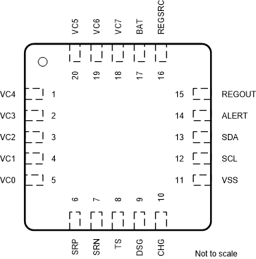
 Figure 5-1 BQ77307 Pinout
Table 5-1 BQ77307 Pin Functions
| PIN | I/O | TYPE | DESCRIPTION | |
|---|---|---|---|---|
| NO. | NAME | |||
| 1 | VC4 | I | IA | Sense voltage input pin for the fourth cell from the bottom of the stack |
| 2 | VC3 | I | IA | Sense voltage input pin for the third cell from the bottom of the stack |
| 1 | VC2 | I | IA | Sense voltage input pin for the second cell from the bottom of the stack |
| 2 | VC1 | I | IA | Sense voltage input pin for the first cell from the bottom of the stack |
| 3 | VC0 | I | IA | Sense voltage input pin for negative terminal of the first cell from the bottom of stack and functions as wakeup from SHUTDOWN |
| 6 | SRP | I | IA | Analog input pin connected to the internal current protection subsystem, which detects a voltage between SRP and SRN, where SRP is the top of the sense resistor. A charging current generates a positive voltage at SRP relative to SRN. |
| 7 | SRN | I | IA | Analog input pin connected to the internal current protection subsystem, which detects a small voltage between SRP and SRN, where SRN is the bottom of the sense resistor. A charging current generates a positive voltage at SRP relative to SRN. |
| 8 | TS | I/O | I/OA | Thermistor input and functions as wakeup from SHUTDOWN |
| 9 | DSG | O | OA | NMOS Discharge FET drive output pin |
| 10 | CHG | O | OA | NMOS Charge FET drive output pin |
| 11 | VSS | — | P | Device ground |
| 12 | SCL | I/O | I/OD | I2C serial communication bus clock |
| 13 | SDA | I/O | I/OD | I2C serial communication bus data |
| 14 | ALERT | O | OD | Digital interrupt output pin |
| 15 | REGOUT | O | OA | LDO output, which can be programmed for 1.8 V, 2.5 V, 3.0 V, 3.3 V, or 5.0 V |
| 16 | REGSRC | I | IA | Input pin for REGOUT LDO also functions as a supply for the CHG and DSG FET drivers. |
| 17 | BAT | I | P | Primary power supply input pin |
| 18 | VC7 | I | IA | Sense voltage input pin for the seventh cell from the bottom of the stack |
| 19 | VC6 | I | IA | Sense voltage input pin for the sixth cell from the bottom of the stack |
| 20 | VC5 | I | IA | Sense voltage input pin for the fifth cell from the bottom of the stack |