SLUSCM3K June 2016 – July 2020 BQ77904 , BQ77905
PRODUCTION DATA
- 1 Features
- 2 Applications
- 3 Description
- 4 Revision History
- 5 Device Comparison
- 6 Pin Configuration and Functions
- 7 Specifications
-
8 Detailed Description
- 8.1 Overview
- 8.2 Functional Block Diagram
- 8.3
Feature Description
- 8.3.1 Protection Summary
- 8.3.2
Fault Operation
- 8.3.2.1 Operation in OV
- 8.3.2.2 Operation in UV
- 8.3.2.3 Operation in OW
- 8.3.2.4 Operation in OCD1
- 8.3.2.5 Operation in OCD2
- 8.3.2.6 Operation in SCD
- 8.3.2.7 Overcurrent Recovery Timer
- 8.3.2.8 Load Removal Detection
- 8.3.2.9 Load Removal Detection in UV
- 8.3.2.10 Operation in OTC
- 8.3.2.11 Operation in OTD
- 8.3.2.12 Operation in UTC
- 8.3.2.13 Operation in UTD
- 8.3.3 Protection Response and Recovery Summary
- 8.3.4 Configuration CRC Check and Comparator Built-In-Self-Test
- 8.3.5 Fault Detection Method
- 8.3.6 State Comparator
- 8.3.7 DSG FET Driver Operation
- 8.3.8 CHG FET Driver Operation
- 8.3.9 External Override of CHG and DSG Drivers
- 8.3.10 Configuring 3-S, 4-S, or 5-S Mode
- 8.3.11 Stacking Implementations
- 8.3.12 Zero-Volt Battery Charging Inhibition
- 8.4 Device Functional Modes
- 9 Application and Implementation
- 10Power Supply Recommendations
- 11Layout
- 12Device and Documentation Support
- 13Mechanical, Packaging, and Orderable Information
Package Options
Mechanical Data (Package|Pins)
- PW|20
Thermal pad, mechanical data (Package|Pins)
Orderable Information
3 Description
The BQ77904 and BQ77905 devices are low-power battery pack protectors that implement a suite of voltage, current, and temperature protections without microcontroller (MCU) control. The device's stackable interface provides simple scaling to support battery cell applications from 3 series to 20 series or more. Protection thresholds and delays are factory-programmed and available in a variety of configurations. Separate overtemperature and undertemperature thresholds for discharge (OTD and UTD) and charge (OTC and UTC) are provided for added flexibility.
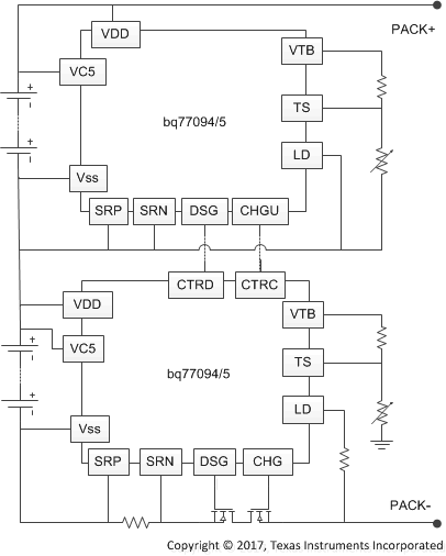
The device achieves pack protection through the integrated independent CHG and DSG low-side NMOS FET drivers, which may be disabled through two control pins. These control pins may also be used to achieve cell protection solutions for higher series (6 series and beyond) in a simple and economical manner. To do this, simply cascade a higher device CHG and DSG outputs to the immediate lower device control pins. For a reduced component count, all protection faults use internal delay timers.
| PART NUMBER(1) | PACKAGE | BODY SIZE (NOM) |
|---|---|---|
| BQ77904 | TSSOP (20) | 6.50 mm × 4.40 mm |
| BQ77905 |
 Simplified Schematic