SLUSF21 june 2023 BQ79616
PRODUCTION DATA
- 1
- 1 Features
- 2 Applications
- 3 Description
- 4 Revision History
- 5 Description (continued)
- 6 Pin Configuration and Functions
- 7 Specifications
-
8 Detailed Description
- 8.1 Overview
- 8.2 Functional Block Diagram
- 8.3
Feature Description
- 8.3.1 Power Supplies
- 8.3.2 Measurement System
- 8.3.3 Cell Balancing
- 8.3.4 Integrated Hardware Protectors
- 8.3.5 GPIO Configuration
- 8.3.6
Communication, OTP, Diagnostic Control
- 8.3.6.1
Communication
- 8.3.6.1.1 Serial Interface
- 8.3.6.1.2 Daisy Chain Interface
- 8.3.6.1.3 Start Communication
- 8.3.6.1.4 Communication Timeout
- 8.3.6.1.5 Communication Debug Mode
- 8.3.6.1.6 Multidrop Configuration
- 8.3.6.1.7 SPI Controller
- 8.3.6.1.8 SPI Loopback
- 8.3.6.2 Fault Handling
- 8.3.6.3 Nonvolatile Memory
- 8.3.6.4 Diagnostic Control/Status
- 8.3.6.1
Communication
- 8.3.7 Bus Bar Support
- 8.4 Device Functional Modes
- 8.5
Register Maps
- 8.5.1 OTP Shadow Register Summary
- 8.5.2 Read/Write Register Summary
- 8.5.3 Read-Only Register Summary
- 8.5.4
Register Field Descriptions
- 8.5.4.1 Device Addressing Setup
- 8.5.4.2 Device ID and Scratch Pad
- 8.5.4.3
General Configuration and Control
- 8.5.4.3.1 DEV_CONF
- 8.5.4.3.2 ACTIVE_CELL
- 8.5.4.3.3 BBVC_POSN1
- 8.5.4.3.4 BBVC_POSN2
- 8.5.4.3.5 PWR_TRANSIT_CONF
- 8.5.4.3.6 COMM_TIMEOUT_CONF
- 8.5.4.3.7 TX_HOLD_OFF
- 8.5.4.3.8 STACK_RESPONSE
- 8.5.4.3.9 BBP_LOC
- 8.5.4.3.10 COMM_CTRL
- 8.5.4.3.11 CONTROL1
- 8.5.4.3.12 CONTROL2
- 8.5.4.3.13 CUST_CRC_HI
- 8.5.4.3.14 CUST_CRC_LO
- 8.5.4.3.15 CUST_CRC_RSLT_HI
- 8.5.4.3.16 CUST_CRC_RSLT_LO
- 8.5.4.4 Operation Status
- 8.5.4.5 ADC Configuration and Control
- 8.5.4.6
ADC Measurement Results
- 8.5.4.6.1 VCELL16_HI/LO
- 8.5.4.6.2 VCELL15_HI/LO
- 8.5.4.6.3 VCELL14_HI/LO
- 8.5.4.6.4 VCELL13_HI/LO
- 8.5.4.6.5 VCELL12_HI/LO
- 8.5.4.6.6 VCELL11_HI/LO
- 8.5.4.6.7 VCELL10_HI/LO
- 8.5.4.6.8 VCELL9_HI/LO
- 8.5.4.6.9 VCELL8_HI/LO
- 8.5.4.6.10 VCELL7_HI/LO
- 8.5.4.6.11 VCELL6_HI/LO
- 8.5.4.6.12 VCELL5_HI/LO
- 8.5.4.6.13 VCELL4_HI/LO
- 8.5.4.6.14 VCELL3_HI/LO
- 8.5.4.6.15 VCELL2_HI/LO
- 8.5.4.6.16 VCELL1_HI/LO
- 8.5.4.6.17 BUSBAR_HI/LO
- 8.5.4.6.18 TSREF_HI/LO
- 8.5.4.6.19 GPIO1_HI/LO
- 8.5.4.6.20 GPIO2_HI/LO
- 8.5.4.6.21 GPIO3_HI/LO
- 8.5.4.6.22 GPIO4_HI/LO
- 8.5.4.6.23 GPIO5_HI/LO
- 8.5.4.6.24 GPIO6_HI/LO
- 8.5.4.6.25 GPIO7_HI/LO
- 8.5.4.6.26 GPIO8_HI/LO
- 8.5.4.6.27 DIETEMP1_HI/LO
- 8.5.4.6.28 DIETEMP2_HI/LO
- 8.5.4.6.29 AUX_CELL_HI/LO
- 8.5.4.6.30 AUX_GPIO_HI/LO
- 8.5.4.6.31 AUX_BAT_HI/LO
- 8.5.4.6.32 AUX_REFL_HI/LO
- 8.5.4.6.33 AUX_VBG2_HI/LO
- 8.5.4.6.34 AUX_AVAO_REF_HI/LO
- 8.5.4.6.35 AUX_AVDD_REF_HI/LO
- 8.5.4.6.36 AUX_OV_DAC_HI/LO
- 8.5.4.6.37 AUX_UV_DAC_HI/LO
- 8.5.4.6.38 AUX_OT_OTCB_DAC_HI/LO
- 8.5.4.6.39 AUX_UT_DAC_HI/LO
- 8.5.4.6.40 AUX_VCBDONE_DAC_HI/LO
- 8.5.4.6.41 AUX_VCM_HI/LO
- 8.5.4.6.42 REFOVDAC_HI/LO
- 8.5.4.6.43 DIAG_MAIN_HI/LO
- 8.5.4.6.44 DIAG_AUX_HI/LO
- 8.5.4.7 Balancing Configuration, Control and Status
- 8.5.4.8 Protector Configuration and Control
- 8.5.4.9 GPIO Configuration
- 8.5.4.10 SPI Controller
- 8.5.4.11 Diagnostic Control
- 8.5.4.12 Fault Configuration and Reset
- 8.5.4.13
Fault Status
- 8.5.4.13.1 FAULT_SUMMARY
- 8.5.4.13.2 FAULT_COMM1
- 8.5.4.13.3 FAULT_COMM2
- 8.5.4.13.4 FAULT_COMM3
- 8.5.4.13.5 FAULT_OTP
- 8.5.4.13.6 FAULT_SYS
- 8.5.4.13.7 FAULT_PROT1
- 8.5.4.13.8 FAULT_PROT2
- 8.5.4.13.9 FAULT_OV1
- 8.5.4.13.10 FAULT_OV2
- 8.5.4.13.11 FAULT_UV1
- 8.5.4.13.12 FAULT_UV2
- 8.5.4.13.13 FAULT_OT
- 8.5.4.13.14 FAULT_UT
- 8.5.4.13.15 FAULT_COMP_GPIO
- 8.5.4.13.16 FAULT_COMP_VCCB1
- 8.5.4.13.17 FAULT_COMP_VCCB2
- 8.5.4.13.18 FAULT_COMP_VCOW1
- 8.5.4.13.19 FAULT_COMP_VCOW2
- 8.5.4.13.20 FAULT_COMP_CBOW1
- 8.5.4.13.21 FAULT_COMP_CBOW2
- 8.5.4.13.22 FAULT_COMP_CBFET1
- 8.5.4.13.23 FAULT_COMP_CBFET2
- 8.5.4.13.24 FAULT_COMP_MISC
- 8.5.4.13.25 FAULT_PWR1
- 8.5.4.13.26 FAULT_PWR2
- 8.5.4.13.27 FAULT_PWR3
- 8.5.4.14
Debug Control and Status
- 8.5.4.14.1 DEBUG_CTRL_UNLOCK
- 8.5.4.14.2 DEBUG_COMM_CTRL1
- 8.5.4.14.3 DEBUG_COMM_CTRL2
- 8.5.4.14.4 DEBUG_COMM_STAT
- 8.5.4.14.5 DEBUG_UART_RC
- 8.5.4.14.6 DEBUG_UART_RR_TR
- 8.5.4.14.7 DEBUG_COMH_BIT
- 8.5.4.14.8 DEBUG_COMH_RC
- 8.5.4.14.9 DEBUG_COMH_RR_TR
- 8.5.4.14.10 DEBUG_COML_BIT
- 8.5.4.14.11 DEBUG_COML_RC
- 8.5.4.14.12 DEBUG_COML_RR_TR
- 8.5.4.14.13 DEBUG_UART_DISCARD
- 8.5.4.14.14 DEBUG_COMH_DISCARD
- 8.5.4.14.15 DEBUG_COML_DISCARD
- 8.5.4.14.16 DEBUG_UART_VALID_HI/LO
- 8.5.4.14.17 DEBUG_COMH_VALID_HI/LO
- 8.5.4.14.18 DEBUG_COML_VALID_HI/LO
- 8.5.4.14.19 DEBUG_OTP_SEC_BLK
- 8.5.4.14.20 DEBUG_OTP_DED_BLK
- 8.5.4.15
OTP Programming Control and Status
- 8.5.4.15.1 OTP_PROG_UNLOCK1A through OTP_PROG_UNLOCK1D
- 8.5.4.15.2 OTP_PROG_UNLOCK2A through OTP_PROG_UNLOCK2D
- 8.5.4.15.3 OTP_PROG_CTRL
- 8.5.4.15.4 OTP_ECC_TEST
- 8.5.4.15.5 OTP_ECC_DATAIN1 through OTP_ECC_DATAIN9
- 8.5.4.15.6 OTP_ECC_DATAOUT1 through OTP_ECC_DATAOUT9
- 8.5.4.15.7 OTP_PROG_STAT
- 8.5.4.15.8 OTP_CUST1_STAT
- 8.5.4.15.9 OTP_CUST2_STAT
-
9 Application and Implementation
- 9.1 Application Information
- 9.2
Typical Applications
- 9.2.1
Base Device Application Circuit
- 9.2.1.1 Design Requirements
- 9.2.1.2 Detailed Design Procedure
- 9.2.1.3 Application Curve
- 9.2.2 Daisy Device Application Circuit
- 9.2.1
Base Device Application Circuit
- 10Power Supply Recommendations
- 11Layout
- 12Device and Documentation Support
- 13Mechanical, Packaging, and Orderable Information
Package Options
Mechanical Data (Package|Pins)
- PAP|64
Thermal pad, mechanical data (Package|Pins)
- PAP|64
Orderable Information
11.1.1 Ground Planes
It is very important to establish a clean grounding scheme to ensure best performance of the device. There are three ground pins (AVSS, DVSS, CVSS) for the device’s internal power supplies and one ground reference (REFHM) for the precision reference. There are noisy grounds and quiet grounds that must be separated in the layout initially and rejoined together in a lower PCB layer. The external components (for example, bypass capacitors) must be tied to the proper grounding group if possible to keep the separation of noisy and quiet grounds apart.
- AVSS ground:
- Bypass capacitor for these pins: BAT, VC0, CB0, and AVDD.
- Package power pad
- DVSS ground:
- Bypass capacitor for DVDD.
- GPIO filter capacitor (if used). It can also connect to AVSS ground plane, if needed.
- CVSS ground:
- Bypass capacitor for GPIOs, CVDD, TSREF, NEG5V, LDOIN, COMHP/N, and COMLP/N.
- REFHM ground:
- Bypass capacitor for REFHP.
- If possible, separate out REFHM from AVSS on the signal connection layer and reconnect REFHM to AVSS ground plane in the lower layer.
Even on a PCB layer that is mainly for signal routing, it is good practice to have a small island of ground pour if possible to provide a low-impedance ground, rather than simply a via through the ground trace to an lower ground plane.
 Figure 11-1 Grounding Layout
Consideration
Figure 11-1 Grounding Layout
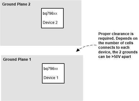
ConsiderationIf multiple devices are placed on the same PCB, each device must have its own ground plane with proper layout clearance.
 Figure 11-2 Separate Ground Planes Per Device on the Same PCB