SBOS030C August 2000 – March 2024 BUF634
PRODUCTION DATA
- 1
- 1 Features
- 2 Applications
- 3 Description
- 4 Device Comparison Table
- 5 Pin Configuration and Functions
-
6 Specifications
- 6.1 Absolute Maximum Ratings
- 6.2 ESD Ratings
- 6.3 Recommended Operating Conditions
- 6.4 Thermal Information
- 6.5 Electrical Characteristics: TO-220 and TO-263 Packages
- 6.6 Electrical Characteristics: Wide-Bandwidth Mode for SOIC Package
- 6.7 Electrical Characteristics: Low-Quiescent-Current Mode for SOIC Package
- 6.8 Typical Characteristics: TO-220 and TO-263 Packages
- 6.9 Typical Characteristics: SOIC Package
- 7 Detailed Description
- 8 Application and Implementation
- 9 Device and Documentation Support
- 10Revision History
- 11Mechanical, Packaging, and Orderable Information
Package Options
Refer to the PDF data sheet for device specific package drawings
Mechanical Data (Package|Pins)
- D|8
- KTT|5
- KC|5
Thermal pad, mechanical data (Package|Pins)
- KTT|5
Orderable Information
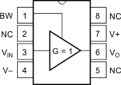
5 Pin Configuration and Functions
 Figure 5-1 D Package, 8-Pin SOIC (Top
View)
 Figure 5-3 KTT Package, 5-Pin TO-263
(Top View)
 Figure 5-2 KC Package, 5-Pin TO-220
(Top View)
Figure 5-2 KC Package, 5-Pin TO-220
(Top View)Table 5-1 Pin Functions
| PIN | TYPE | DESCRIPTION | ||
|---|---|---|---|---|
| NAME | NO. | |||
| D (SOIC) | KC (TO-220) KTT (TO-263) |
|||
| BW | 1 | 1 | Input | Bandwidth adjust pin |
| NC | 2, 5, 8 | — | — | No internal connection |
| V+ | 7 | 5 | Input | Positive power supply |
| VIN | 3 | 2 | Input | Input |
| VO | 6 | 4 | Output | Output |
| V– | 4 | 3 | Input | Negative power supply |