SBOS030C August 2000 – March 2024 BUF634
PRODUCTION DATA
- 1
- 1 Features
- 2 Applications
- 3 Description
- 4 Device Comparison Table
- 5 Pin Configuration and Functions
-
6 Specifications
- 6.1 Absolute Maximum Ratings
- 6.2 ESD Ratings
- 6.3 Recommended Operating Conditions
- 6.4 Thermal Information
- 6.5 Electrical Characteristics: TO-220 and TO-263 Packages
- 6.6 Electrical Characteristics: Wide-Bandwidth Mode for SOIC Package
- 6.7 Electrical Characteristics: Low-Quiescent-Current Mode for SOIC Package
- 6.8 Typical Characteristics: TO-220 and TO-263 Packages
- 6.9 Typical Characteristics: SOIC Package
- 7 Detailed Description
- 8 Application and Implementation
- 9 Device and Documentation Support
- 10Revision History
- 11Mechanical, Packaging, and Orderable Information
Package Options
Refer to the PDF data sheet for device specific package drawings
Mechanical Data (Package|Pins)
- D|8
- KTT|5
- KC|5
Thermal pad, mechanical data (Package|Pins)
- KTT|5
Orderable Information
8.1 Application Information
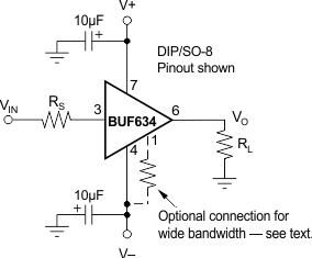
Figure 8-1 shows the BUF634 device connected as an open-loop buffer. The source impedance and optional input resistor, RS, influence frequency response: see Section 6.8. Bypass power supplies with capacitors connected close to the device pins. Capacitor values as low as 0.1 µF provide stable operation in most applications, but high output current and fast output slewing can demand large current transients from the power supplies. Solid tantalum 10-µF capacitors are recommended. High-frequency, open-loop applications can benefit from special bypassing and layout considerations. For more information, see Section 8.1.1.
 Figure 8-1 Buffer Connections