SBOS998C June 2021 – March 2022 BUF802
PRODUCTION DATA
- 1 Features
- 2 Applications
- 3 Description
- 4 Revision History
- 5 Pin Configuration and Functions
- 6 Specifications
- 7 Parameter Measurement Information
- 8 Detailed Description
- 9 Application and Implementation
- 10Power Supply Recommendations
- 11Layout
- 12Device and Documentation Support
- 13Mechanical, Packaging, and Orderable Information
Package Options
Mechanical Data (Package|Pins)
- RGT|16
Thermal pad, mechanical data (Package|Pins)
- RGT|16
Orderable Information
8.4.2 Composite Loop Mode (CL Mode)
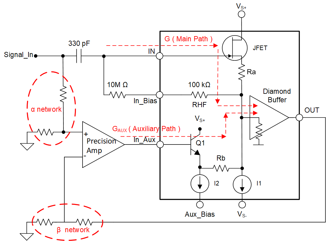
 Figure 8-12 Internal Schematic – CL
Mode
 Figure 8-13 CL
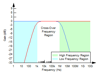
Mode Frequency Response
Figure 8-13 CL
Mode Frequency ResponseThe 330 pF input series capacitor shown in Figure 8-12 splits the input signal into a low-frequency and high-frequency component. These signals are applied to In_Aux and IN respectively. The IN pin controls the output of BUF802 through the Main Path, whereas the In_Aux pin controls the output through the Auxiliary Path.
The transfer function of the composite loop in CL Mode can be split into the following 3 frequency regions:
- Low Frequency Region: The gain of the composite loop in the low-frequency region is α/β (determined by α and β network). In the low-frequency region the 330 pF input capacitor presents a high-impedance in the Main Path, causing the signal to flow through the precision amplifier and the In_Aux pin. This region spans from DC to fLF. fLF is the pole resulting from the gain bandwidth of the precision amplifier, the Auxiliary Path bandwidth, and parasitic capacitance of the components along the path.
- High Frequency Region: In the high-frequency region, the precision amplifier and the Auxiliary Path run out of bandwidth. The net gain of the composite loop in this region is determined solely by the Main Path gain of the BUF802, which is denoted by G. This region spans from the pole created at fHF till the LSBW of the BUF802. The fHF is the pole resulting from the 330 pF series capacitor and the 10 MΩ resistor on the In_Bias pin.
- Cross-over Frequency
Region: the Main Path and Auxiliary Path work in conjunction to
determine the gain in the crossover region. To maintain a flat frequency
response in this region, the following conditions have to be met:
- α/β = G
- High frequency response pole fHF<< Low frequency pole fLF