SWRS293 November   2023 CC1312PSIP

PRODUCTION DATA  

  1.   1
  2. Features
  3. Applications
  4. Description
  5. Functional Block Diagram
  6. Revision History
  7. Device Comparison
  8. Pin Configuration and Functions
    1. 7.1 Pin Diagram – MOT Package (Top View)
    2. 7.2 Signal Descriptions – MOT Package
    3. 7.3 Connections for Unused Pins and Modules
  9. Specifications
    1. 8.1  Absolute Maximum Ratings
    2. 8.2  ESD Ratings
    3. 8.3  Recommended Operating Conditions
    4. 8.4  Power Supply and Modules
    5. 8.5  Power Consumption - Power Modes
    6. 8.6  Power Consumption - Radio Modes
    7. 8.7  Nonvolatile (Flash) Memory Characteristics
    8. 8.8  Thermal Resistance Characteristics
    9. 8.9  RF Frequency Bands
    10. 8.10 861 MHz to 1054 MHz - Receive (RX)
    11. 8.11 861 MHz to 1054 MHz - Transmit (TX) 
    12. 8.12 861 MHz to 1054 MHz - PLL Phase Noise Wideband Mode
    13. 8.13 861 MHz to 1054 MHz - PLL Phase Noise Narrowband Mode
    14. 8.14 Timing and Switching Characteristics
      1. 8.14.1 Reset Timing
      2. 8.14.2 Wakeup Timing
      3. 8.14.3 Clock Specifications
        1. 8.14.3.1 48 MHz Crystal Oscillator (XOSC_HF) and RF frequency accuracy
        2. 8.14.3.2 48 MHz RC Oscillator (RCOSC_HF)
        3. 8.14.3.3 2 MHz RC Oscillator (RCOSC_MF)
        4. 8.14.3.4 32.768 kHz Crystal Oscillator (XOSC_LF) and RTC accuracy
        5. 8.14.3.5 32 kHz RC Oscillator (RCOSC_LF)
      4. 8.14.4 Synchronous Serial Interface (SSI) Characteristics
        1.       36
          1. 8.14.4.1.1 Synchronous Serial Interface (SSI) Characteristics
      5. 8.14.5 UART
        1. 8.14.5.1 UART Characteristics
    15. 8.15 Peripheral Characteristics
      1. 8.15.1 ADC
        1. 8.15.1.1 Analog-to-Digital Converter (ADC) Characteristics
      2. 8.15.2 DAC
        1. 8.15.2.1 Digital-to-Analog Converter (DAC) Characteristics
      3. 8.15.3 Temperature and Battery Monitor
        1. 8.15.3.1 Temperature Sensor
        2. 8.15.3.2 Battery Monitor
      4. 8.15.4 Comparators
        1. 8.15.4.1 Low-Power Clocked Comparator
        2. 8.15.4.2 Continuous Time Comparator
      5. 8.15.5 Current Source
        1. 8.15.5.1 Programmable Current Source
      6. 8.15.6 GPIO
        1. 8.15.6.1 GPIO DC Characteristics
    16. 8.16 Typical Characteristics
      1. 8.16.1 MCU Current
      2. 8.16.2 RX Current
      3. 8.16.3 TX Current
      4. 8.16.4 RX Performance
      5. 8.16.5 TX Performance
      6. 8.16.6 ADC Performance
      7. 8.16.7 Temperature Compensation
  10. Detailed Description
    1. 9.1  Overview
    2. 9.2  System CPU
    3. 9.3  Radio (RF Core)
      1. 9.3.1 Proprietary Radio Formats
    4. 9.4  Memory
    5. 9.5  Sensor Controller
    6. 9.6  Cryptography
    7. 9.7  Timers
    8. 9.8  Serial Peripherals and I/O
    9. 9.9  Battery and Temperature Monitor
    10. 9.10 µDMA
    11. 9.11 Debug
    12. 9.12 Power Management
    13. 9.13 Clock Systems, production calibration and temperature compensation
    14. 9.14 Network Processor
    15. 9.15 Device Certification and Qualification
      1. 9.15.1 FCC Certification and Statement
      2. 9.15.2 IC/ISED Certification and Statement
    16. 9.16 Module Markings
    17. 9.17 End Product Labeling
    18. 9.18 Manual Information to the End User
  11. 10Application, Implementation, and Layout
    1. 10.1 Application Information
      1. 10.1.1 Typical Application Circuit
    2. 10.2 Device Connection and Layout Fundamentals
      1. 10.2.1 Reset
      2. 10.2.2 Unused Pins
    3. 10.3 PCB Layout Guidelines
      1. 10.3.1 General Layout Recommendations
      2. 10.3.2 RF Layout Recommendations
        1. 10.3.2.1 Antenna Placement and Routing
        2. 10.3.2.2 Transmission Line Considerations
    4. 10.4 Reference Designs
  12. 11Environmental Requirements and SMT Specifications
    1. 11.1 PCB Bending
    2. 11.2 Handling Environment
      1. 11.2.1 Terminals
      2. 11.2.2 Falling
    3. 11.3 Storage Condition
      1. 11.3.1 Moisture Barrier Bag Before Opened
      2. 11.3.2 Moisture Barrier Bag Open
    4. 11.4 PCB Assembly Guide
      1. 11.4.1 PCB Land Pattern & Thermal Vias
      2. 11.4.2 SMT Assembly Recommendations
      3. 11.4.3 PCB Surface Finish Requirements
      4. 11.4.4 Solder Stencil
      5. 11.4.5 Package Placement
      6. 11.4.6 Solder Joint Inspection
      7. 11.4.7 Rework and Replacement
      8. 11.4.8 Solder Joint Voiding
    5. 11.5 Baking Conditions
    6. 11.6 Soldering and Reflow Condition
  13. 12Device and Documentation Support
    1. 12.1 Device Nomenclature
    2. 12.2 Tools and Software
      1. 12.2.1 SimpleLink™ Microcontroller Platform
    3. 12.3 Documentation Support
    4. 12.4 Support Resources
    5. 12.5 Trademarks
    6. 12.6 Electrostatic Discharge Caution
    7. 12.7 Glossary
  14. 13Mechanical, Packaging, and Orderable Information

Package Options

Mechanical Data (Package|Pins)
Thermal pad, mechanical data (Package|Pins)
Orderable Information

Mechanical, Packaging, and Orderable Information

The following pages include mechanical packaging and orderable information. This information is the most current data available for the designated devices. This data is subject to change without notice and revision of this document. For browser-based versions of this data sheet, refer to the left-hand navigation.

Note:

The total height of the module is 1.51 mm.

The weight of the CC1312PSIP module is typically 0.19 g.
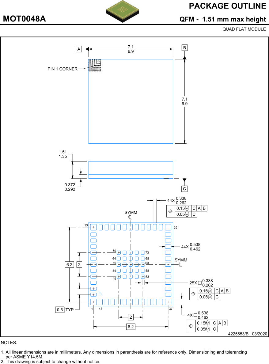
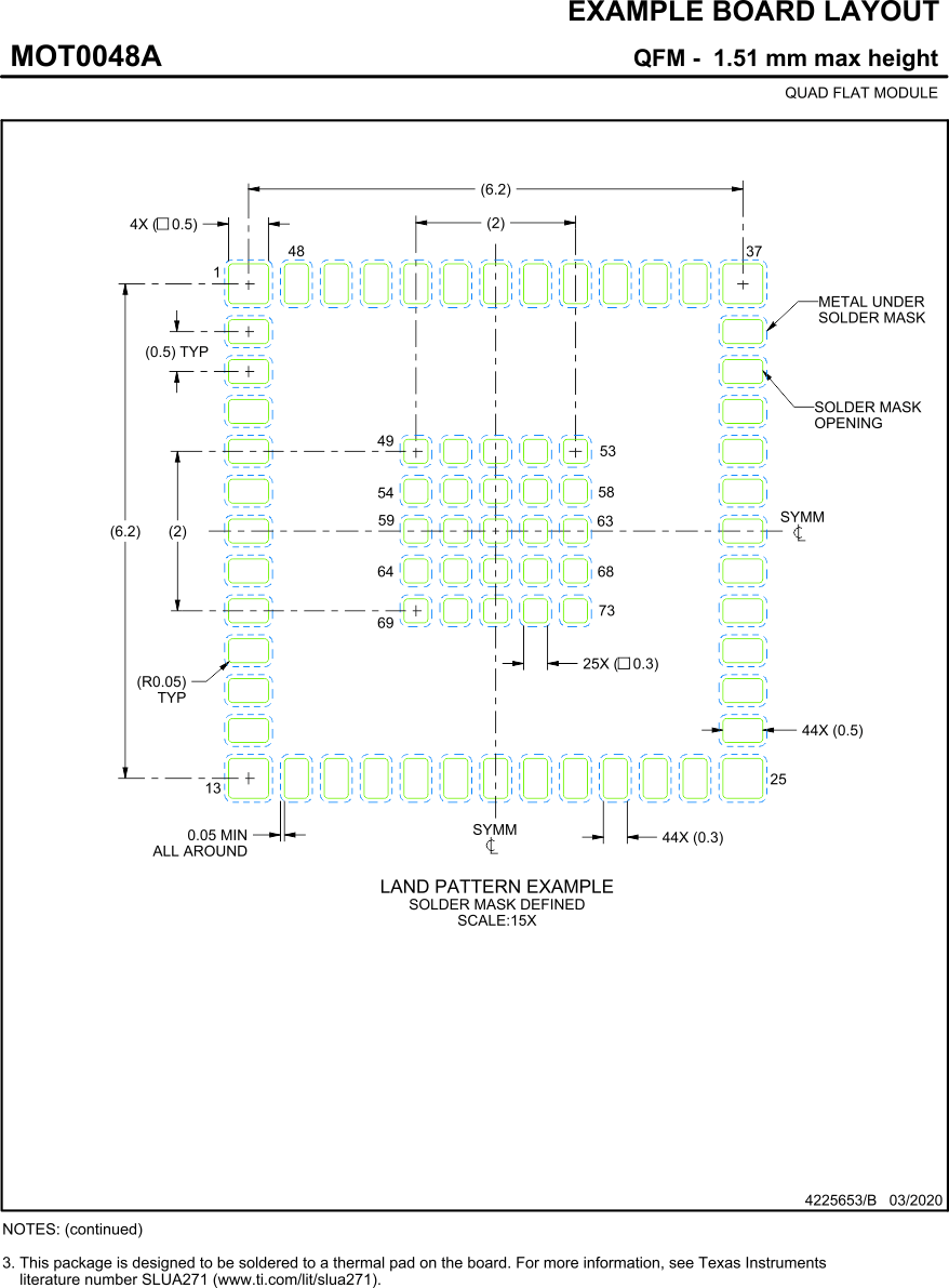
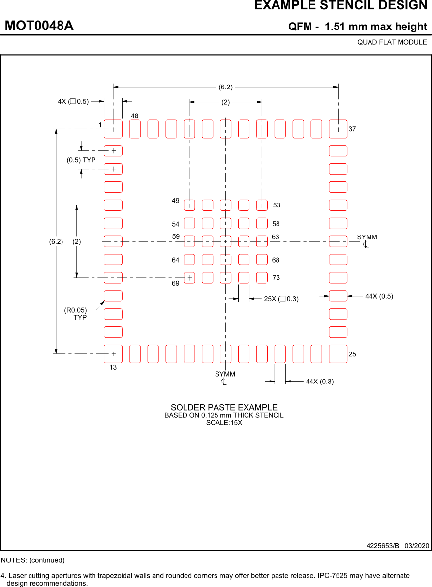
GUID-20201016-CA0I-DHCM-FWWD-ML3P2521HBNB-low.gif
GUID-20201016-CA0I-DZCG-R8WL-L3TG88RXBHRM-low.gif
GUID-20201016-CA0I-VCR7-WRQG-XVV2KK9KMK5D-low.gif