SWRS293 November 2023 CC1312PSIP
PRODUCTION DATA
- 1
- 1 Features
- 2 Applications
- 3 Description
- 4 Functional Block Diagram
- 5 Revision History
- 6 Device Comparison
- 7 Pin Configuration and Functions
-
8 Specifications
- 8.1 Absolute Maximum Ratings
- 8.2 ESD Ratings
- 8.3 Recommended Operating Conditions
- 8.4 Power Supply and Modules
- 8.5 Power Consumption - Power Modes
- 8.6 Power Consumption - Radio Modes
- 8.7 Nonvolatile (Flash) Memory Characteristics
- 8.8 Thermal Resistance Characteristics
- 8.9 RF Frequency Bands
- 8.10 861 MHz to 1054 MHz - Receive (RX)
- 8.11 861 MHz to 1054 MHz - Transmit (TX)
- 8.12 861 MHz to 1054 MHz - PLL Phase Noise Wideband Mode
- 8.13 861 MHz to 1054 MHz - PLL Phase Noise Narrowband Mode
- 8.14 Timing and Switching Characteristics
- 8.15 Peripheral Characteristics
- 8.16 Typical Characteristics
-
9 Detailed Description
- 9.1 Overview
- 9.2 System CPU
- 9.3 Radio (RF Core)
- 9.4 Memory
- 9.5 Sensor Controller
- 9.6 Cryptography
- 9.7 Timers
- 9.8 Serial Peripherals and I/O
- 9.9 Battery and Temperature Monitor
- 9.10 µDMA
- 9.11 Debug
- 9.12 Power Management
- 9.13 Clock Systems, production calibration and temperature compensation
- 9.14 Network Processor
- 9.15 Device Certification and Qualification
- 9.16 Module Markings
- 9.17 End Product Labeling
- 9.18 Manual Information to the End User
- 10Application, Implementation, and Layout
- 11Environmental Requirements and SMT Specifications
- 12Device and Documentation Support
- 13Mechanical, Packaging, and Orderable Information
Package Options
Mechanical Data (Package|Pins)
- MOT|48
Thermal pad, mechanical data (Package|Pins)
Orderable Information
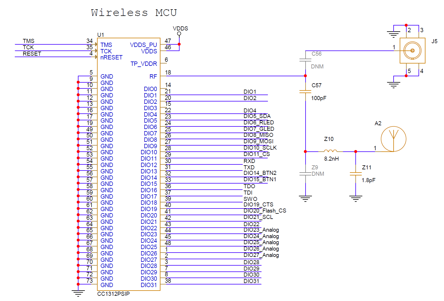
10.1.1 Typical Application Circuit
Figure 10-1 shows the typical application schematic using the CC1312PSIP module. For the full reference schematic, download the LP-EM-CC1312PSIP Design Files.
The following guidelines are recommended for implementation of the RF design:
- Ensure an RF path is designed with a characteristic impedance of 50 Ω.
- Tuning of the antenna impedance matching network is recommended after manufacturing of the PCB to account for PCB parasitics. Please refer to CC13xx/CC26xx Hardware Configuration and PCB Design Considerations; section 5.1 for further information.
 Figure 10-1 CC1312PSIP Typical Application Schematic with integrated antenna on LP-EM-CC1312PSIP
Table 10-1 provides the bill of materials for a typical application using the CC1312PSIP module in Figure 10-1.
It is always recommended to insert a pi-filter (Z9, Z10 and Z11) between the RF pad and the antenna / SMA connector. When matching towards an antenna, this will minimize the mismatch losses of the antenna. A low-pass match or high-pass matching network can typically be chosen.
For the CC1312PSIP, it is recommended to use a low-pass antenna match since this will both match the antenna but will also act as a low-pass filter function as well. As can be seen in Figure 10-1, Z10 and Z11 form a low-pass antenna match on the LP-EM-CC1312PSIP that has an integrated PCB antenna.
For 902-915 MHz only, in the event that no matching components are required for the antenna or direct connection to a SMA, it is recommended to just to use a DC blocking capacitor of 100 pF. For operation at both 868/869 MHz and 902-928 MHz, then it is also recommended to use an LC filter of Z10: 3.9 nH and Z11: 3.6 pF as a low-pass filter.
For full operation reference design, see the LP-EM-CC1312PSIP Design Files.
| QTY | PART REFERENCE | VALUE | MANUFACTURER | PART NUMBER | DESCRIPTION |
|---|---|---|---|---|---|
| 1 | C57 | 100pF | Murata | GRM0335C1H101GA01D | Capacitor, Ceramic C0G/NP0, 100pF, 50V, -2%/+2%, -55DEGC/+125DEGC, 0201, SMD |
| 1 | U1 | CC1312PSIP | Texas Instruments | CC1312PSIP | IC, CC1312PSIP, LGA73, SMD |
| 1 | Z10 | 8.2nH | Murata | LQP03TN8N2J02D | Inductor, RF, Chip, Non-magnetic core, 8.2nH, -5%/+5%, 0.25A, -55DEGC/+125DEGC, 0201, SMD |
| 1 | Z11 | 1.8pF | Murata | GRM0335C1H1R8BA01J | Capacitor, Ceramic C0G/NP0, 1.8pF, 50V, -0.1pF/+0.1pF, -55DEGC/+125DEGC, 0201, SMD |