SWRS178C February 2015 – July 2016 CC2620
PRODUCTION DATA.
- 1Device Overview
- 2Revision History
- 3 Device Comparison
- 4Terminal Configuration and Functions
-
5Specifications
- 5.1 Absolute Maximum Ratings
- 5.2 ESD Ratings
- 5.3 Recommended Operating Conditions
- 5.4 Power Consumption Summary
- 5.5 General Characteristics
- 5.6 IEEE 802.15.4 (Offset Q-PSK DSSS, 250 kbps) - RX
- 5.7 IEEE 802.15.4 (Offset Q-PSK DSSS, 250 kbps) - TX
- 5.8 24-MHz Crystal Oscillator (XOSC_HF)
- 5.9 32.768-kHz Crystal Oscillator (XOSC_LF)
- 5.10 48-MHz RC Oscillator (RCOSC_HF)
- 5.11 32-kHz RC Oscillator (RCOSC_LF)
- 5.12 ADC Characteristics
- 5.13 Temperature Sensor
- 5.14 Battery Monitor
- 5.15 Continuous Time Comparator
- 5.16 Low-Power Clocked Comparator
- 5.17 Programmable Current Source
- 5.18 Synchronous Serial Interface (SSI)
- 5.19 DC Characteristics
- 5.20 Thermal Resistance Characteristics
- 5.21 Timing Requirements
- 5.22 Switching Characteristics
- 5.23 Typical Characteristics
- 6Detailed Description
- 7Application, Implementation, and Layout
- 8Device and Documentation Support
- 9Mechanical Packaging and Orderable Information
Package Options
Mechanical Data (Package|Pins)
Thermal pad, mechanical data (Package|Pins)
Orderable Information
4 Terminal Configuration and Functions
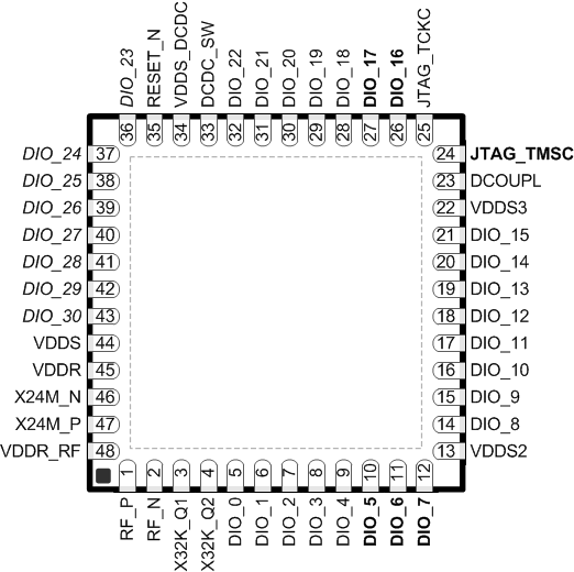
4.1 Pin Diagram – RGZ Package

NOTE:
I/O pins marked in bold have high drive capabilities. I/O pins marked in italics have analog capabilities.48-Pin VQFN
(7-mm × 7-mm) Pinout, 0.5-mm Pitch
4.2 Signal Descriptions – RGZ Package
Table 4-1 Signal Descriptions – RGZ Package
| NAME | NO. | TYPE | DESCRIPTION |
|---|---|---|---|
| DCDC_SW | 33 | Power | Output from internal DC-DC(1) |
| DCOUPL | 23 | Power | 1.27-V regulated digital-supply decoupling capacitor(2) |
| DIO_0 | 5 | Digital I/O | GPIO, Sensor Controller |
| DIO_1 | 6 | Digital I/O | GPIO, Sensor Controller |
| DIO_2 | 7 | Digital I/O | GPIO, Sensor Controller |
| DIO_3 | 8 | Digital I/O | GPIO, Sensor Controller |
| DIO_4 | 9 | Digital I/O | GPIO, Sensor Controller |
| DIO_5 | 10 | Digital I/O | GPIO, Sensor Controller, high-drive capability |
| DIO_6 | 11 | Digital I/O | GPIO, Sensor Controller, high-drive capability |
| DIO_7 | 12 | Digital I/O | GPIO, Sensor Controller, high-drive capability |
| DIO_8 | 14 | Digital I/O | GPIO |
| DIO_9 | 15 | Digital I/O | GPIO |
| DIO_10 | 16 | Digital I/O | GPIO |
| DIO_11 | 17 | Digital I/O | GPIO |
| DIO_12 | 18 | Digital I/O | GPIO |
| DIO_13 | 19 | Digital I/O | GPIO |
| DIO_14 | 20 | Digital I/O | GPIO |
| DIO_15 | 21 | Digital I/O | GPIO |
| DIO_16 | 26 | Digital I/O | GPIO, JTAG_TDO, high-drive capability |
| DIO_17 | 27 | Digital I/O | GPIO, JTAG_TDI, high-drive capability |
| DIO_18 | 28 | Digital I/O | GPIO |
| DIO_19 | 29 | Digital I/O | GPIO |
| DIO_20 | 30 | Digital I/O | GPIO |
| DIO_21 | 31 | Digital I/O | GPIO |
| DIO_22 | 32 | Digital I/O | GPIO |
| DIO_23 | 36 | Digital/Analog I/O | GPIO, Sensor Controller, Analog |
| DIO_24 | 37 | Digital/Analog I/O | GPIO, Sensor Controller, Analog |
| DIO_25 | 38 | Digital/Analog I/O | GPIO, Sensor Controller, Analog |
| DIO_26 | 39 | Digital/Analog I/O | GPIO, Sensor Controller, Analog |
| DIO_27 | 40 | Digital/Analog I/O | GPIO, Sensor Controller, Analog |
| DIO_28 | 41 | Digital/Analog I/O | GPIO, Sensor Controller, Analog |
| DIO_29 | 42 | Digital/Analog I/O | GPIO, Sensor Controller, Analog |
| DIO_30 | 43 | Digital/Analog I/O | GPIO, Sensor Controller, Analog |
| JTAG_TMSC | 24 | Digital I/O | JTAG TMSC, high-drive capability |
| JTAG_TCKC | 25 | Digital I/O | JTAG TCKC |
| RESET_N | 35 | Digital input | Reset, active-low. No internal pullup. |
| RF_P | 1 | RF I/O | Positive RF input signal to LNA during RX Positive RF output signal to PA during TX |
| RF_N | 2 | RF I/O | Negative RF input signal to LNA during RX Negative RF output signal to PA during TX |
| VDDR | 45 | Power | 1.7-V to 1.95-V supply, typically connect to output of internal DC-DC(2)(3) |
| VDDR_RF | 48 | Power | 1.7-V to 1.95-V supply, typically connect to output of internal DC-DC(2)(4) |
| VDDS | 44 | Power | 1.8-V to 3.8-V main chip supply(1) |
| VDDS2 | 13 | Power | 1.8-V to 3.8-V DIO supply(1) |
| VDDS3 | 22 | Power | 1.8-V to 3.8-V DIO supply(1) |
| VDDS_DCDC | 34 | Power | 1.8-V to 3.8-V DC-DC supply |
| X32K_Q1 | 3 | Analog I/O | 32-kHz crystal oscillator pin 1 |
| X32K_Q2 | 4 | Analog I/O | 32-kHz crystal oscillator pin 2 |
| X24M_N | 46 | Analog I/O | 24-MHz crystal oscillator pin 1 |
| X24M_P | 47 | Analog I/O | 24-MHz crystal oscillator pin 2 |
| EGP | Power | Ground – Exposed Ground Pad | |
(1) See technical reference manual (listed in Section 8.3) for more details.
(2) Do not supply external circuitry from this pin.
(3) If internal DC-DC is not used, this pin is supplied internally from the main LDO.
(4) If internal DC-DC is not used, this pin must be connected to VDDR for supply from the main LDO.
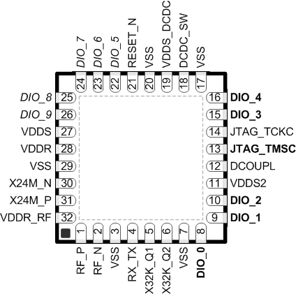
4.3 Pin Diagram – RSM Package

NOTE:
I/O pins marked in bold have high drive capabilities. I/O pins marked in italics have analog capabilities.32-Pin VQFN
(4-mm × 4-mm) Pinout, 0.4-mm Pitch
4.4 Signal Descriptions – RSM Package
Table 4-2 Signal Descriptions – RSM Package
| NAME | NO. | TYPE | DESCRIPTION |
|---|---|---|---|
| DCDC_SW | 18 | Power | Output from internal DC-DC. (1). Tie to ground for external regulator mode (1.7-V to 1.95-V operation) |
| DCOUPL | 12 | Power | 1.27-V regulated digital-supply decoupling capacitor(2) |
| DIO_0 | 8 | Digital I/O | GPIO, Sensor Controller, high-drive capability |
| DIO_1 | 9 | Digital I/O | GPIO, Sensor Controller, high-drive capability |
| DIO_2 | 10 | Digital I/O | GPIO, Sensor Controller, high-drive capability |
| DIO_3 | 15 | Digital I/O | GPIO, High drive capability, JTAG_TDO |
| DIO_4 | 16 | Digital I/O | GPIO, High drive capability, JTAG_TDI |
| DIO_5 | 22 | Digital/Analog I/O | GPIO, Sensor Controller, Analog |
| DIO_6 | 23 | Digital/Analog I/O | GPIO, Sensor Controller, Analog |
| DIO_7 | 24 | Digital/Analog I/O | GPIO, Sensor Controller, Analog |
| DIO_8 | 25 | Digital/Analog I/O | GPIO, Sensor Controller, Analog |
| DIO_9 | 26 | Digital/Analog I/O | GPIO, Sensor Controller, Analog |
| JTAG_TMSC | 13 | Digital I/O | JTAG TMSC |
| JTAG_TCKC | 14 | Digital I/O | JTAG TCKC |
| RESET_N | 21 | Digital Input | Reset, active-low. No internal pullup. |
| RF_N | 2 | RF I/O | Negative RF input signal to LNA during RX Negative RF output signal to PA during TX |
| RF_P | 1 | RF I/O | Positive RF input signal to LNA during RX Positive RF output signal to PA during TX |
| RX_TX | 4 | RF I/O | Optional bias pin for the RF LNA |
| VDDR | 28 | Power | 1.7-V to 1.95-V supply, typically connect to output of internal DC-DC. (2)(3) |
| VDDR_RF | 32 | Power | 1.7-V to 1.95-V supply, typically connect to output of internal DC-DC(2)(4) |
| VDDS | 27 | Power | 1.8-V to 3.8-V main chip supply(1) |
| VDDS2 | 11 | Power | 1.8-V to 3.8-V GPIO supply(1) |
| VDDS_DCDC | 19 | Power | 1.8-V to 3.8-V DC-DC supply. Tie to ground for external regulator mode (1.7-V to 1.95-V operation). |
| VSS | 3, 7, 17, 20, 29 | Power | Ground |
| X32K_Q1 | 5 | Analog I/O | 32-kHz crystal oscillator pin 1 |
| X32K_Q2 | 6 | Analog I/O | 32-kHz crystal oscillator pin 2 |
| X24M_N | 30 | Analog I/O | 24-MHz crystal oscillator pin 1 |
| X24M_P | 31 | Analog I/O | 24-MHz crystal oscillator pin 2 |
| EGP | Power | Ground – Exposed Ground Pad | |
(1) See technical reference manual (listed in Section 8.3) for more details.
(2) Do not supply external circuitry from this pin.
(3) If internal DC-DC is not used, this pin is supplied internally from the main LDO.
(4) If internal DC-DC is not used, this pin must be connected to VDDR for supply from the main LDO.