SWAS034B February   2017  – July 2024 CC3120

PRODUCTION DATA  

  1.   1
  2. Features
  3. Applications
  4. Description
  5. Functional Block Diagrams
  6. Device Comparison
    1. 5.1 Related Products
  7. Terminal Configuration and Functions
    1. 6.1 Pin Diagram
    2. 6.2 Pin Attributes
    3. 6.3 Connections for Unused Pins
  8. Specifications
    1. 7.1  Absolute Maximum Ratings
    2. 7.2  ESD Ratings
    3. 7.3  Power-On Hours (POH)
    4. 7.4  Recommended Operating Conditions
    5. 7.5  Current Consumption Summary
    6. 7.6  TX Power and IBAT versus TX Power Level Settings
    7. 7.7  Brownout and Blackout Conditions
    8. 7.8  Electrical Characteristics (3.3 V, 25°C)
    9. 7.9  WLAN Receiver Characteristics
    10. 7.10 WLAN Transmitter Characteristics
    11. 7.11 WLAN Filter Requirements
      1. 7.11.1 WLAN Filter Requirements
    12. 7.12 Thermal Resistance Characteristics
      1. 7.12.1 Thermal Resistance Characteristics for RGK Package
    13. 7.13 Reset Requirement
    14. 7.14 Timing and Switching Characteristics
      1. 7.14.1 Power Supply Sequencing
      2. 7.14.2 Device Reset
      3. 7.14.3 Reset Timing
        1. 7.14.3.1 nRESET (32-kHz Crystal)
        2. 7.14.3.2 First-Time Power-Up and Reset Removal Timing Requirements (32-kHz Crystal)
        3. 7.14.3.3 nRESET (External 32-kHz)
          1. 7.14.3.3.1 First-Time Power-Up and Reset Removal Timing Requirements (External 32-kHz)
      4. 7.14.4 Wakeup From HIBERNATE Mode
        1. 7.14.4.1 nHIB Timing Requirements
      5. 7.14.5 Clock Specifications
        1. 7.14.5.1 Slow Clock Using Internal Oscillator
          1. 7.14.5.1.1 RTC Crystal Requirements
        2. 7.14.5.2 Slow Clock Using an External Clock
          1. 7.14.5.2.1 External RTC Digital Clock Requirements
        3. 7.14.5.3 Fast Clock (Fref) Using an External Crystal
          1. 7.14.5.3.1 WLAN Fast-Clock Crystal Requirements
        4. 7.14.5.4 Fast Clock (Fref) Using an External Oscillator
          1. 7.14.5.4.1 External Fref Clock Requirements (–40°C to +85°C)
      6. 7.14.6 Interfaces
        1. 7.14.6.1 Host SPI Interface Timing
          1. 7.14.6.1.1 Host SPI Interface Timing Parameters
        2. 7.14.6.2 Flash SPI Interface Timing
          1. 7.14.6.2.1 Flash SPI Interface Timing Parameters
    15. 7.15 External Interfaces
      1. 7.15.1 SPI Flash Interface
        1. 7.15.1.1 SPI Flash Interface
      2. 7.15.2 SPI Host Interface
        1. 7.15.2.1 SPI Host Interface
      3. 7.15.3 Host UART Interface
        1. 7.15.3.1 SimpleLink™ UART Configuration
        2. 7.15.3.2 5-Wire UART Topology
        3. 7.15.3.3 4-Wire UART Topology
        4. 7.15.3.4 3-Wire UART Topology
  9. Detailed Description
    1. 8.1 Device Features
      1. 8.1.1 WLAN
      2. 8.1.2 Network Stack
      3. 8.1.3 Security
      4. 8.1.4 Host Interface and Driver
      5. 8.1.5 System
    2. 8.2 Power-Management Subsystem
      1. 8.2.1 VBAT Wide-Voltage Connection
      2. 8.2.2 Preregulated 1.85V
    3. 8.3 Low-Power Operating Modes
      1. 8.3.1 Low-Power Deep Sleep
      2. 8.3.2 Hibernate
      3. 8.3.3 Shutdown
    4. 8.4 Memory
      1. 8.4.1 External Memory Requirements
    5. 8.5 Restoring Factory Default Configuration
  10. Applications, Implementation, and Layout
    1. 9.1 Application Information
      1. 9.1.1 Typical Application—CC3120R Wide-Voltage Mode
      2. 9.1.2 Typical Application Schematic—CC3120R Preregulated, 1.85-V Mode
    2. 9.2 PCB Layout Guidelines
      1. 9.2.1 General PCB Guidelines
      2. 9.2.2 Power Layout and Routing
        1. 9.2.2.1 Design Considerations
      3. 9.2.3 Clock Interfaces
      4. 9.2.4 Digital Input and Output
      5. 9.2.5 RF Interface
  11. 10Device and Documentation Support
    1. 10.1 Development Tools and Software
    2. 10.2 Firmware Updates
    3. 10.3 Device Nomenclature
    4. 10.4 Documentation Support
    5. 10.5 Support Resources
    6. 10.6 Trademarks
    7. 10.7 Electrostatic Discharge Caution
    8. 10.8 Export Control Notice
    9. 10.9 Glossary
  12. 11Revision History
  13. 12Mechanical, Packaging, and Orderable Information
    1. 12.1 Packaging Information

Package Options

Mechanical Data (Package|Pins)
Thermal pad, mechanical data (Package|Pins)
Orderable Information

nRESET (External 32-kHz)

Figure 7-7 shows the reset timing diagram for the external 32-kHz first-time power-up and reset removal.
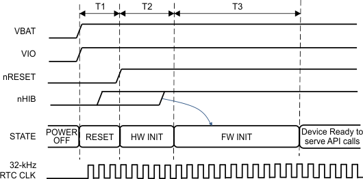
CC3120 First-Time Power-Up and Reset Removal Timing Diagram (External 32-kHz)Figure 7-7 First-Time Power-Up and Reset Removal Timing Diagram (External 32-kHz)


Section 7.14.3.3.1 describes the timing requirements for the external first-time power-up and reset removal.