SWAS037C February   2019  – December 2024 CC3135

PRODUCTION DATA  

  1.   1
  2. Features
  3. Applications
  4. Description
  5. Functional Block Diagram
  6. Device Comparison
    1. 5.1 Related Products
  7. Pin Configuration and Functions
    1. 6.1 Pin Diagram
    2. 6.2 Pin Attributes
    3. 6.3 Signal Descriptions
      1.      12
    4. 6.4 Connections for Unused Pins
  8. Specifications
    1. 7.1  Absolute Maximum Ratings
    2. 7.2  ESD Ratings
    3. 7.3  Power-On Hours (POH)
    4. 7.4  Recommended Operating Conditions
    5. 7.5  Current Consumption Summary: 2.4 GHz RF Band
    6. 7.6  Current Consumption Summary: 5 GHz RF Band
    7. 7.7  TX Power Control for 2.4 GHz Band
    8. 7.8  TX Power Control for 5 GHz
    9. 7.9  Brownout and Blackout Conditions
      1.      24
    10. 7.10 Electrical Characteristics for DIO Pins
      1.      26
      2.      27
    11. 7.11 Electrical Characteristics for Pin Internal Pullup and Pulldown
    12. 7.12 WLAN Receiver Characteristics
      1.      30
      2.      31
    13. 7.13 WLAN Transmitter Characteristics
      1.      33
      2.      34
    14. 7.14 WLAN Transmitter Out-of-Band Emissions
      1.      36
      2.      37
    15. 7.15 BLE/2.4 GHz Radio Coexistence and WLAN Coexistence Requirements
    16. 7.16 Thermal Resistance Characteristics for RGK Package
    17. 7.17 Timing and Switching Characteristics
      1. 7.17.1 Power Supply Sequencing
      2. 7.17.2 Device Reset
      3. 7.17.3 Reset Timing
        1. 7.17.3.1 nRESET (32-kHz Crystal)
        2.       45
        3. 7.17.3.2 nRESET (External 32-kHz Crystal)
          1.        47
      4. 7.17.4 Wakeup From HIBERNATE Mode
        1.       49
      5. 7.17.5 Clock Specifications
        1. 7.17.5.1 Slow Clock Using Internal Oscillator
          1.        52
        2. 7.17.5.2 Slow Clock Using an External Clock
          1.        54
        3. 7.17.5.3 Fast Clock (Fref) Using an External Crystal
          1.        56
        4. 7.17.5.4 Fast Clock (Fref) Using an External Oscillator
          1.        58
      6. 7.17.6 Interfaces
        1. 7.17.6.1 Host SPI Interface Timing
          1.        61
        2. 7.17.6.2 Flash SPI Interface Timing
          1.        63
        3. 7.17.6.3 DIO Interface Timing
          1. 7.17.6.3.1 DIO Output Transition Time Parameters (Vsupply = 3.3 V)
            1.         66
          2. 7.17.6.3.2 DIO Input Transition Time Parameters
            1.         68
    18. 7.18 External Interfaces
      1. 7.18.1 SPI Flash Interface
      2. 7.18.2 SPI Host Interface
      3. 7.18.3 Host UART Interface
        1. 7.18.3.1 5-Wire UART Topology
        2. 7.18.3.2 4-Wire UART Topology
        3. 7.18.3.3 3-Wire UART Topology
  9. Detailed Description
    1. 8.1 Overview
    2. 8.2 Device Features
      1. 8.2.1 WLAN
      2. 8.2.2 Network Stack
      3. 8.2.3 Security
      4. 8.2.4 Host Interface and Driver
      5. 8.2.5 System
    3. 8.3 FIPS 140-2 Level 1 Certification
    4. 8.4 Power-Management Subsystem
      1. 8.4.1 VBAT Wide-Voltage Connection
    5. 8.5 Low-Power Operating Modes
      1. 8.5.1 Low-Power Deep Sleep
      2. 8.5.2 Hibernate
      3. 8.5.3 Shutdown
    6. 8.6 Memory
      1. 8.6.1 External Memory Requirements
    7. 8.7 Restoring Factory Default Configuration
    8. 8.8 Hostless Mode
  10. Applications, Implementation, and Layout
    1. 9.1 Application Information
      1. 9.1.1 BLE/2.4GHz Radio Coexistence
      2. 9.1.2 Antenna Selection
      3. 9.1.3 Typical Application
    2. 9.2 PCB Layout Guidelines
      1. 9.2.1 General PCB Guidelines
      2. 9.2.2 Power Layout and Routing
        1. 9.2.2.1 Design Considerations
      3. 9.2.3 Clock Interface Guidelines
      4. 9.2.4 Digital Input and Output Guidelines
      5. 9.2.5 RF Interface Guidelines
  11. 10Device and Documentation Support
    1. 10.1  Third-Party Products Disclaimer
    2. 10.2  Tools and Software
    3. 10.3  Firmware Updates
    4. 10.4  Device Nomenclature
    5. 10.5  Documentation Support
    6. 10.6  Support Resources
    7. 10.7  Trademarks
    8. 10.8  Electrostatic Discharge Caution
    9. 10.9  Export Control Notice
    10. 10.10 Glossary
  12. 11Revision History
  13. 12Mechanical, Packaging, and Orderable Information
    1. 12.1 Packaging Information
    2. 12.2 Tape and Reel Information

Package Options

Mechanical Data (Package|Pins)
Thermal pad, mechanical data (Package|Pins)
Orderable Information

TX Power Control for 2.4 GHz Band

The CC3135 has several options for modifying the output power of the device when required. For the 2.4 GHz band it is possible to lower the overall output power at a global level using the global TX power level setting. In addition, the 2.4 GHz band allows the user to enter additional back-offs (1), per channel, region (2)and modulation rates (3), via Image creator (see the UniFlash CC31xx, CC32xx SimpleLink™ Wi-Fi® and Internet-on-a chip™ Solution ImageCreator and Programming Tool User's Guide for more details).

Figure 7-1, Figure 7-2, and Figure 7-3 show TX power and IBAT versus TX power level settings for the CC3135 device at modulations of 1 DSSS, 6 OFDM, and 54 OFDM, respectively.

In Figure 7-1, the area enclosed in the circle represents a significant reduction in current during transition from TX power level 3 to level 4. In the case of lower range requirements (14-dBm output power), TI recommends using TX power level 4 to reduce the current.
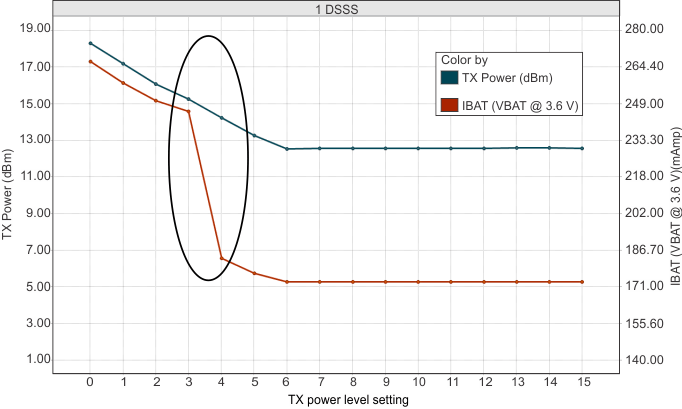
CC3135 TX Power and IBAT vs TX Power Level Settings (1 DSSS)Figure 7-1 TX Power and IBAT vs TX Power Level Settings (1 DSSS)
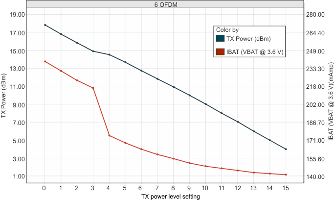


CC3135 TX Power and IBAT vs TX Power Level Settings (6 OFDM)Figure 7-2 TX Power and IBAT vs TX Power Level Settings (6 OFDM)
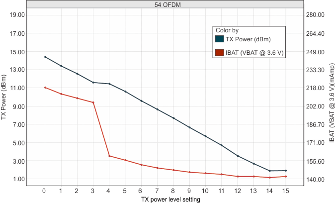
CC3135 TX Power and IBAT vs TX Power Level Settings (54 OFDM)Figure 7-3 TX Power and IBAT vs TX Power Level Settings (54 OFDM)


The back-off range is between -6 dB to +6 dB in 0.25 dB increments.
FCC/ISED, ETSI (Europe), and Japan are supported.
Back-off rates are grouped into 11b rates, high modulation rates (MCS7, 54 OFDM and 48 OFDM), and lower modulation rates (all other rates).