SWRS225D February   2019  – May 2021 CC3135MOD

PRODUCTION DATA  

  1. Features
  2. Applications
  3. Description
  4. Functional Block Diagrams
  5. Revision History
  6. Device Comparison
    1. 6.1 Related Products
  7. Terminal Configuration and Functions
    1. 7.1 CC3135MOD Pin Diagram
    2. 7.2 Pin Attributes
    3. 7.3 Signal Descriptions
      1.      12
    4. 7.4 Connections for Unused Pins
  8. Specifications
    1. 8.1  Absolute Maximum Ratings
    2. 8.2  ESD Ratings
    3. 8.3  Recommended Operating Conditions
    4. 8.4  Current Consumption Summary: 2.4 GHz RF Band
    5. 8.5  Current Consumption Summary: 5 GHz RF Band
    6. 8.6  TX Power Control for 2.4 GHz Band
    7. 8.7  TX Power Control for 5 GHz Band
    8. 8.8  Brownout and Blackout Conditions
    9. 8.9  Electrical Characteristics for DIO Pins
    10. 8.10 WLAN Receiver Characteristics
      1.      25
      2.      26
    11. 8.11 WLAN Transmitter Characteristics
      1.      28
      2.      29
    12. 8.12 BLE and WLAN Coexistence Requirements
    13. 8.13 Reset Requirement
    14. 8.14 Thermal Resistance Characteristics for MOB Package
    15. 8.15 Timing and Switching Characteristics
      1. 8.15.1 Power-Up Sequencing
      2. 8.15.2 Power-Down Sequencing
      3. 8.15.3 Device Reset
      4. 8.15.4 Wakeup From HIBERNATE Mode Timing
    16. 8.16 External Interfaces
      1. 8.16.1 SPI Host Interface
      2. 8.16.2 Host UART Interface
        1. 8.16.2.1 5-Wire UART Topology
        2. 8.16.2.2 4-Wire UART Topology
        3. 8.16.2.3 3-Wire UART Topology
      3. 8.16.3 External Flash Interface
  9. Detailed Description
    1. 9.1  Overview
    2. 9.2  Module Features
      1. 9.2.1 WLAN
      2. 9.2.2 Network Stack
        1. 9.2.2.1 Security
      3. 9.2.3 FIPS 140-2 Level 1 Certification
      4. 9.2.4 Host Interface and Driver
      5. 9.2.5 System
    3. 9.3  Power-Management Subsystem
      1. 9.3.1 VBAT Wide-Voltage Connection
    4. 9.4  Low-Power Operating Modes
      1. 9.4.1 Low-Power Deep Sleep
      2. 9.4.2 Hibernate
      3. 9.4.3 Shutdown
    5. 9.5  Restoring Factory Default Configuration
    6. 9.6  Hostless Mode
    7. 9.7  Device Certification and Qualification
      1. 9.7.1 FCC Certification and Statement
      2. 9.7.2 IC/ISED Certification Statement
      3. 9.7.3 ETSI/CE Certification
      4. 9.7.4 Japan MIC Certification
    8. 9.8  Module Markings
    9. 9.9  End Product Labeling
    10. 9.10 Manual Information to the End User
  10. 10Applications, Implementation, and Layout
    1. 10.1 Application Information
      1. 10.1.1 BLE/2.4 GHz Radio Coexistence
      2. 10.1.2 Antenna Selection
      3. 10.1.3 Typical Application
      4. 10.1.4 Power Supply Decoupling and Bulk Capacitors
      5. 10.1.5 Reset
      6. 10.1.6 Unused Pins
    2. 10.2 PCB Layout Guidelines
      1. 10.2.1 General Layout Recommendations
      2. 10.2.2 RF Layout Recommendations
      3. 10.2.3 Antenna Placement and Routing
      4. 10.2.4 Transmission Line Considerations
  11. 11Environmental Requirements and SMT Specifications
    1. 11.1 Temperature
      1. 11.1.1 PCB Bending
    2. 11.2 Handling Environment
      1. 11.2.1 Terminals
      2. 11.2.2 Falling
    3. 11.3 Storage Condition
      1. 11.3.1 Moisture Barrier Bag Before Opened
      2. 11.3.2 Moisture Barrier Bag Open
    4. 11.4 PCB Assembly Guide
      1. 11.4.1 PCB Land Pattern & Thermal Vias
      2. 11.4.2 SMT Assembly Recommendations
      3. 11.4.3 PCB Surface Finish Requirements
      4. 11.4.4 Solder Stencil
      5. 11.4.5 Package Placement
      6. 11.4.6 Solder Joint Inspection
      7. 11.4.7 Rework and Replacement
      8. 11.4.8 Solder Joint Voiding
    5. 11.5 Baking Conditions
    6. 11.6 Soldering and Reflow Condition
  12. 12Device and Documentation Support
    1. 12.1 Device Nomenclature
    2. 12.2 Development Tools and Software
    3. 12.3 Firmware Updates
    4. 12.4 Documentation Support
    5. 12.5 Trademarks
    6. 12.6 Electrostatic Discharge Caution
    7. 12.7 Export Control Notice
    8. 12.8 Glossary
  13. 13Mechanical, Packaging, and Orderable Information
    1. 13.1 Mechanical, Land, and Solder Paste Drawings
    2. 13.2 Package Option Addendum
      1. 13.2.1 Packaging Information
      2. 13.2.2 Tape and Reel Information
        1. 13.2.2.1 Tape Specifications

Package Options

Mechanical Data (Package|Pins)
Thermal pad, mechanical data (Package|Pins)

Antenna Selection

The CC3135MOD device is designed to also support antenna selection and is controlled from Image Creator. When enabled, there are 3 options possible options:

  • ANT 1: When selected, the GPIOs that are defined for antenna selection with set the RF path for antenna 1.
  • ANT 2: When selected, the GPIOs that are defined for antenna selection will set the RF path for antenna 2.
  • Autoselect: When selected, during a scan and prior to connecting to an AP, CC3135MOD device will determine the best RF path and select the appropriate antenna (12)(13). The result is the saved as port of the profile.

Figure 10-2 shows the antenna selection implementation for Wi-Fi, with BLE operating on it's own antenna. Note in this implementation, only a single GPIO from the BLE device to the CC3135MOD device is required. The Antenna switch (14)is controlled by 2 GPIO lines from the CC3135MOD device. Table 7-2 lists which GPIOs can be used for Antenna Selection.
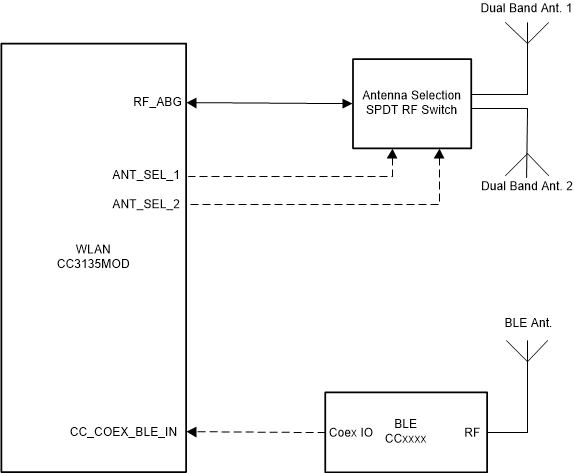
GUID-BD50B2F0-C7AD-4D5A-B244-7D691B0DAEE3-low.gif Figure 10-2 Coexistence Solution with Wi-Fi Antenna Selection and dedicated BLE antenna
When selecting Autoselect via the API, a reset is required in order for the CC3135MOD device to determine the best antenna for use.
Refer to the Uniflash with Image Creator User Guidefor more information.
The recommended Antenna switch is the Richwave RTC6608OSP.