SWRS225E February   2019  – December 2024 CC3135MOD

PRODUCTION DATA  

  1.   1
  2. Features
  3. Applications
  4. Description
  5. Functional Block Diagrams
  6. Device Comparison
    1. 5.1 Related Products
  7. Pin Configuration and Functions
    1. 6.1 CC3135MOD Pin Diagram
    2. 6.2 Pin Attributes
    3. 6.3 Signal Descriptions
      1.      12
    4. 6.4 Connections for Unused Pins
  8. Specifications
    1. 7.1  Absolute Maximum Ratings
    2. 7.2  ESD Ratings
    3. 7.3  Recommended Operating Conditions
    4. 7.4  Current Consumption Summary: 2.4GHz RF Band
    5. 7.5  Current Consumption Summary: 5GHz RF Band
    6. 7.6  TX Power Control for 2.4 GHz Band
    7. 7.7  TX Power Control for 5GHz Band
    8. 7.8  Brownout and Blackout Conditions
    9. 7.9  Electrical Characteristics for DIO Pins
    10. 7.10 WLAN Receiver Characteristics
      1.      25
      2.      26
    11. 7.11 WLAN Transmitter Characteristics
      1.      28
      2.      29
    12. 7.12 BLE and WLAN Coexistence Requirements
    13. 7.13 Reset Requirement
    14. 7.14 Thermal Resistance Characteristics for MOB Package
    15. 7.15 Timing and Switching Characteristics
      1. 7.15.1 Power-Up Sequencing
      2. 7.15.2 Power-Down Sequencing
      3. 7.15.3 Device Reset
      4. 7.15.4 Wakeup From HIBERNATE Mode Timing
    16. 7.16 External Interfaces
      1. 7.16.1 SPI Host Interface
      2. 7.16.2 Host UART Interface
        1. 7.16.2.1 5-Wire UART Topology
        2. 7.16.2.2 4-Wire UART Topology
        3. 7.16.2.3 3-Wire UART Topology
      3. 7.16.3 External Flash Interface
  9. Detailed Description
    1. 8.1  Overview
    2. 8.2  Module Features
      1. 8.2.1 WLAN
      2. 8.2.2 Network Stack
        1. 8.2.2.1 Security
      3. 8.2.3 FIPS 140-2 Level 1 Certification
      4. 8.2.4 Host Interface and Driver
      5. 8.2.5 System
    3. 8.3  Power-Management Subsystem
      1. 8.3.1 VBAT Wide-Voltage Connection
    4. 8.4  Low-Power Operating Modes
      1. 8.4.1 Low-Power Deep Sleep
      2. 8.4.2 Hibernate
      3. 8.4.3 Shutdown
    5. 8.5  Restoring Factory Default Configuration
    6. 8.6  Hostless Mode
    7. 8.7  Device Certification and Qualification
      1. 8.7.1 FCC Certification and Statement
      2. 8.7.2 IC/ISED Certification Statement
      3. 8.7.3 ETSI/CE Certification
      4. 8.7.4 Japan MIC Certification
    8. 8.8  Module Markings
    9. 8.9  End Product Labeling
    10. 8.10 Manual Information to the End User
  10. Applications, Implementation, and Layout
    1. 9.1 Application Information
      1. 9.1.1 BLE/2.4 GHz Radio Coexistence
      2. 9.1.2 Antenna Selection
      3. 9.1.3 Typical Application
      4. 9.1.4 Power Supply Decoupling and Bulk Capacitors
      5. 9.1.5 Reset
      6. 9.1.6 Unused Pins
    2. 9.2 PCB Layout Guidelines
      1. 9.2.1 General Layout Recommendations
      2. 9.2.2 RF Layout Recommendations
      3. 9.2.3 Antenna Placement and Routing
      4. 9.2.4 Transmission Line Considerations
  11. 10Environmental Requirements and SMT Specifications
    1. 10.1 Temperature
      1. 10.1.1 PCB Bending
    2. 10.2 Handling Environment
      1. 10.2.1 Terminals
      2. 10.2.2 Falling
    3. 10.3 Storage Condition
      1. 10.3.1 Moisture Barrier Bag Before Opened
      2. 10.3.2 Moisture Barrier Bag Open
    4. 10.4 PCB Assembly Guide
      1. 10.4.1 PCB Land Pattern & Thermal Vias
      2. 10.4.2 SMT Assembly Recommendations
      3. 10.4.3 PCB Surface Finish Requirements
      4. 10.4.4 Solder Stencil
      5. 10.4.5 Package Placement
      6. 10.4.6 Solder Joint Inspection
      7. 10.4.7 Rework and Replacement
      8. 10.4.8 Solder Joint Voiding
    5. 10.5 Baking Conditions
    6. 10.6 Soldering and Reflow Condition
  12. 11Device and Documentation Support
    1. 11.1 Device Nomenclature
    2. 11.2 Development Tools and Software
    3. 11.3 Firmware Updates
    4. 11.4 Documentation Support
    5. 11.5 Trademarks
    6. 11.6 Electrostatic Discharge Caution
    7. 11.7 Export Control Notice
    8. 11.8 Glossary
  13. 12Revision History
  14. 13Mechanical, Packaging, and Orderable Information
    1. 13.1 Mechanical, Land, and Solder Paste Drawings
    2. 13.2 Package Option Addendum
      1. 13.2.1 Packaging Information
      2. 13.2.2 Tape and Reel Information
        1. 13.2.2.1 Tape Specifications

Package Options

Mechanical Data (Package|Pins)
Thermal pad, mechanical data (Package|Pins)

Soldering and Reflow Condition

  • Heating method: Conventional convection or IR convection
  • Temperature measurement: Thermocouple d = 0.1mm to 0.2mm CA (K) or CC (T) at soldering portion or equivalent method
  • Solder paste composition: SAC305
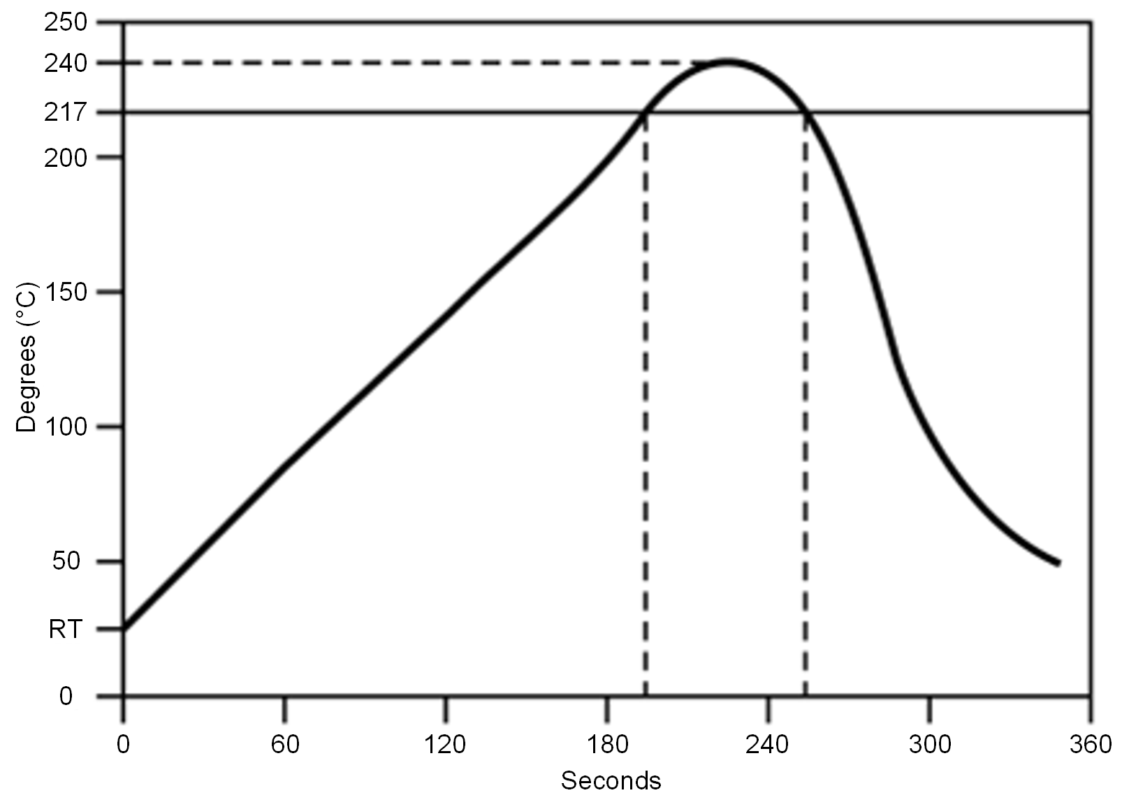
  • Allowable reflow soldering times: 2 times based on the reflow soldering profile (see Figure 10-1)
  • Temperature profile: Reflow soldering will be done according to the temperature profile (see
    Figure 10-1)
  • Peak temp: 260°C
CC3135MOD Temperature Profile for Evaluation of Solder Heat Resistance of a Component (at Solder Joint)Figure 10-1 Temperature Profile for Evaluation of Solder Heat Resistance of a Component (at Solder Joint)
Table 10-1 Temperature Profile
Profile ElementsConvection or IR(1)
Peak temperature range235 to 240°C typical (260°C maximum)
Pre-heat / soaking (150 to 200°C)60 to 120 seconds
Time above melting point60 to 90 seconds
Time with 5°C to peak30 seconds maximum
Ramp up< 3°C / second
Ramp down< -6°C / second
For details, refer to the solder paste manufacturer's recommendation.


Note:

TI does not recommend using conformal coating or similar material on the SimpleLink™ module. This coating can lead to localized stress on the WCSP solder connections inside the module and impact the device's reliability. Use caution during the module assembly process to the final PCB to avoid the presence of foreign material inside the module.