SWAS032F July 2013 – February 2015 CC3200
PRODUCTION DATA.
- 1Device Overview
- 2Revision History
- 3Terminal Configuration and Functions
-
4Specifications
- 4.1 Absolute Maximum Ratings
- 4.2 Handling Ratings
- 4.3 Power-On Hours
- 4.4 Recommended Operating Conditions
- 4.5 Brown-Out and Black-Out
- 4.6 Electrical Characteristics (3.3 V, 25°C)
- 4.7 WLAN Receiver Characteristics
- 4.8 WLAN Transmitter Characteristics
- 4.9 Current Consumption
- 4.10 Thermal Characteristics for RGC Package
- 4.11 Timing and Switching Characteristics
- 5Detailed Description
- 6Applications and Implementation
- 7Device and Documentation Support
- 8Mechanical Packaging and Orderable Information
Package Options
Mechanical Data (Package|Pins)
- RGC|64
Thermal pad, mechanical data (Package|Pins)
- RGC|64
Orderable Information
1 Device Overview
1.1 Features
- CC3200 SimpleLink Wi-Fi—Consists of Applications Microcontroller, Wi-Fi Network Processor, and Power-Management Subsystems
- Wi-Fi CERTIFIED™ Chip
- Applications Microcontroller Subsystem
- ARM®Cortex®-M4 Core at 80 MHz
- Embedded Memory
- RAM (Up to 256KB)
- External Serial Flash Bootloader, and Peripheral Drivers in ROM
- 32-Channel Direct Memory Access (μDMA)
- Hardware Crypto Engine for Advanced Fast Security, Including
- AES, DES, and 3DES
- SHA2 and MD5
- CRC and Checksum
- 8-Bit Parallel Camera Interface
- 1 Multichannel Audio Serial Port (McASP) Interface with Support for Two I2S Channels
- 1 SD/MMC Interface
- 2 Universal Asynchronous Receivers and Transmitters (UARTs)
- 1 Serial Peripheral Interface (SPI)
- 1 Inter-Integrated Circuit (I2C)
- 4 General-Purpose Timers with 16-Bit Pulse-Width Modulation (PWM) Mode
- 1 Watchdog Timer
- 4-Channel 12-Bit Analog-to-Digital Converters (ADCs)
- Up to 27 Individually Programmable, Multiplexed GPIO Pins
- Dedicated External SPI Interface for Serial Flash
- Wi-Fi Network Processor Subsystem
- Featuring Wi-Fi Internet-On-a-Chip™
- Dedicated ARM MCU
- Wi-Fi and Internet Protocols in ROM
- 802.11 b/g/n Radio, Baseband, Medium Access Control (MAC), Wi-Fi Driver, and Supplicant
- TCP/IP Stack
- Industry-Standard BSD Socket Application Programming Interfaces (APIs)
- 8 Simultaneous TCP or UDP Sockets
- 2 Simultaneous TLS and SSL Sockets
- Powerful Crypto Engine for Fast, Secure Wi-Fi and Internet Connections with 256-Bit AES Encryption for TLS and SSL Connections
- Station, AP, and Wi-Fi Direct® Modes
- WPA2 Personal and Enterprise Security
- SimpleLink Connection Manager for Autonomous and Fast Wi-Fi Connections
- SmartConfig™ Technology, AP Mode, and WPS2 for Easy and Flexible Wi-Fi Provisioning
- TX Power
- 18.0 dBm @ 1 DSSS
- 14.5 dBm @ 54 OFDM
- RX Sensitivity
- –95.7 dBm @ 1 DSSS
- –74.0 dBm @ 54 OFDM
- Application Throughput
- UDP: 16 Mbps
- TCP: 13 Mbps
Completely Offloads Wi-Fi and Internet Protocols from the Application Microcontroller
- Power-Management Subsystem
- Integrated DC-DC Supports a Wide Range of Supply Voltage:
- VBAT Wide-Voltage Mode: 2.1 to 3.6 V
- VIO is Always Tied with VBAT
- Preregulated 1.85-V Mode
- Advanced Low-Power Modes
- Integrated DC-DC Supports a Wide Range of Supply Voltage:
- Clock Source
- 40.0-MHz Crystal with Internal Oscillator
- 32.768-kHz Crystal or External RTC Clock
- Package and Operating Temperature
- 0.5-mm Pitch, 64-Pin, 9-mm × 9-mm QFN
- Ambient Temperature Range: –40°C to 85°C
1.2 Applications
- For Internet-of-Things applications, such as:
- Cloud Connectivity
- Home Automation
- Home Appliances
- Access Control
- Security Systems
- Smart Energy
- Internet Gateway
- Industrial Control
- Smart Plug and Metering
- Wireless Audio
- IP Network Sensor Nodes
1.3 Description
Start your design with the industry’s first Wi-Fi CERTIFIED single-chip microcontroller unit (MCU) with built-in Wi-Fi connectivity. Created for the Internet of Things (IoT), the SimpleLink CC3200 device is a wireless MCU that integrates a high-performance ARM Cortex-M4 MCU, allowing customers to develop an entire application with a single IC. With on-chip Wi-Fi, Internet, and robust security protocols, no prior Wi-Fi experience is required for faster development. The CC3200 device is a complete platform solution including software, sample applications, tools, user and programming guides, reference designs, and the TI E2E™ support community. The device is available in a QFN package that is easy to layout.
The applications MCU subsystem contains an industry-standard ARM Cortex-M4 core running at 80 MHz. The device includes a wide variety of peripherals, including a fast parallel camera interface, I2S, SD/MMC, UART, SPI, I2C, and four-channel ADC. The CC3200 family includes flexible embedded RAM for code and data and ROM with external serial flash bootloader and peripheral drivers.
The Wi-Fi network processor subsystem features a Wi-Fi Internet-on-a-Chip and contains an additional dedicated ARM MCU that completely offloads the applications MCU. This subsystem includes an 802.11 b/g/n radio, baseband, and MAC with a powerful crypto engine for fast, secure Internet connections with 256-bit encryption. The CC3200 device supports Station, Access Point, and Wi-Fi Direct modes. The device also supports WPA2 personal and enterprise security and WPS 2.0. The Wi-Fi Internet-on-a-chip includes embedded TCP/IP and TLS/SSL stacks, HTTP server, and multiple Internet protocols.
The power-management subsystem includes integrated DC-DC converters supporting a wide range of supply voltages. This subsystem enables low-power consumption modes, such as the hibernate with RTC mode requiring less than 4 μA of current.
1.4 Functional Block Diagram
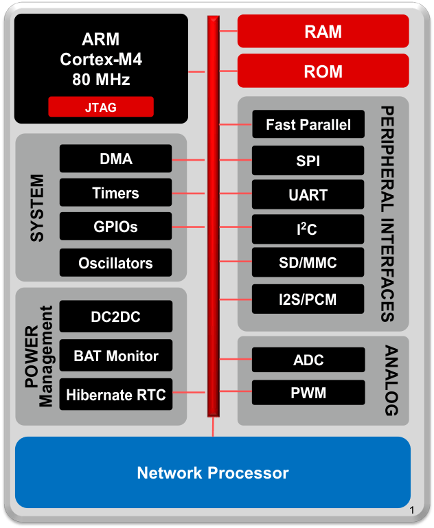
Figure 1-1 shows the CC3200 hardware overview.
 Figure 1-1 CC3200 Hardware Overview
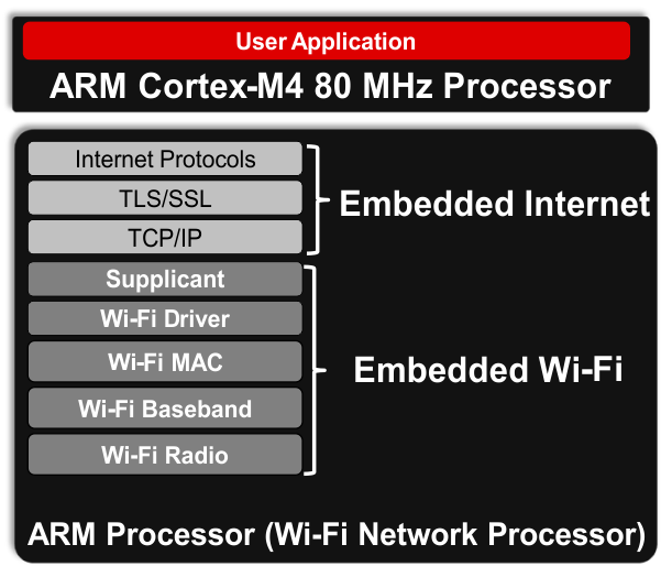
Figure 1-2 shows an overview of the CC3200 embedded software.
 Figure 1-2 CC3200 Embedded Software Overview
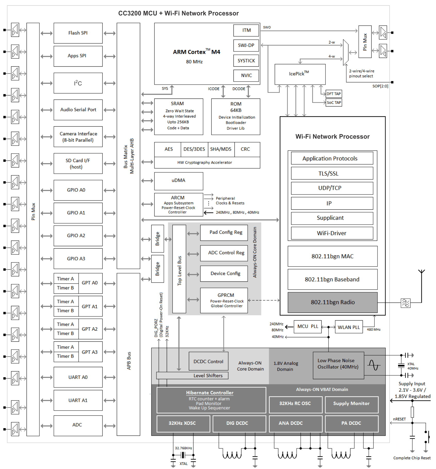
Figure 1-3 shows a block diagram of the CC3200 device.
