SWRS226C February   2020  – December 2024 CC3230S , CC3230SF

PRODUCTION DATA  

  1.   1
  2. Features
  3. Applications
  4. Description
  5. Functional Block Diagrams
  6. Device Comparison
    1. 5.1 Related Products
  7. Terminal Configuration and Functions
    1. 6.1 Pin Diagram
    2. 6.2 Pin Attributes
      1. 6.2.1 Pin Descriptions
    3. 6.3 Signal Descriptions
      1.      13
    4. 6.4 Pin Multiplexing
    5. 6.5 Drive Strength and Reset States for Analog and Digital Multiplexed Pins
    6. 6.6 Pad State After Application of Power to Device, Before Reset Release
    7. 6.7 Connections for Unused Pins
  8. Specifications
    1. 7.1  Absolute Maximum Ratings
    2. 7.2  ESD Ratings
    3. 7.3  Power-On Hours (POH)
    4. 7.4  Recommended Operating Conditions
    5. 7.5  Current Consumption Summary (CC3230S)
      1.      24
    6. 7.6  Current Consumption Summary (CC3230SF)
      1.      26
    7. 7.7  TX Power Control
    8. 7.8  Brownout and Blackout Conditions
    9. 7.9  Electrical Characteristics for GPIO Pins
      1. 7.9.1 Electrical Characteristics: GPIO Pins Except 29, 30, 50, 52, and 53
      2. 7.9.2 Electrical Characteristics: GPIO Pins 29, 30, 50, 52, and 53
    10. 7.10 Electrical Characteristics for Pin Internal Pullup and Pulldown
      1.      33
    11. 7.11 WLAN Receiver Characteristics
      1.      35
    12. 7.12 WLAN Transmitter Characteristics
      1.      37
    13. 7.13 WLAN Transmitter Out-of-Band Emissions
      1. 7.13.1 WLAN Filter Requirements
    14. 7.14 BLE/2.4 GHz Radio Coexistence and WLAN Coexistence Requirements
    15. 7.15 Thermal Resistance Characteristics for RGK Package
    16. 7.16 Timing and Switching Characteristics
      1. 7.16.1 Power Supply Sequencing
      2. 7.16.2 Device Reset
      3. 7.16.3 Reset Timing
        1. 7.16.3.1 nRESET (32-kHz Crystal)
        2. 7.16.3.2 First-Time Power-Up and Reset Removal Timing Requirements (32-kHz Crystal)
        3. 7.16.3.3 nRESET (External 32-kHz Clock)
          1. 7.16.3.3.1 First-Time Power-Up and Reset Removal Timing Requirements (External 32-kHz Clock)
      4. 7.16.4 Wakeup From HIBERNATE Mode
      5. 7.16.5 Clock Specifications
        1. 7.16.5.1 Slow Clock Using Internal Oscillator
        2. 7.16.5.2 Slow Clock Using an External Clock
          1. 7.16.5.2.1 External RTC Digital Clock Requirements
        3. 7.16.5.3 Fast Clock (Fref) Using an External Crystal
          1. 7.16.5.3.1 WLAN Fast-Clock Crystal Requirements
        4. 7.16.5.4 Fast Clock (Fref) Using an External Oscillator
          1. 7.16.5.4.1 External Fref Clock Requirements (–40°C to +85°C)
      6. 7.16.6 Peripherals Timing
        1. 7.16.6.1  SPI
          1. 7.16.6.1.1 SPI Master
            1. 7.16.6.1.1.1 SPI Master Timing Parameters
          2. 7.16.6.1.2 SPI Slave
            1. 7.16.6.1.2.1 SPI Slave Timing Parameters
        2. 7.16.6.2  I2S
          1. 7.16.6.2.1 I2S Transmit Mode
            1. 7.16.6.2.1.1 I2S Transmit Mode Timing Parameters
          2. 7.16.6.2.2 I2S Receive Mode
            1. 7.16.6.2.2.1 I2S Receive Mode Timing Parameters
        3. 7.16.6.3  GPIOs
          1. 7.16.6.3.1 GPIO Output Transition Time Parameters (Vsupply = 3.3 V)
            1. 7.16.6.3.1.1 GPIO Output Transition Times (Vsupply = 3.3 V) #GUID-761098ED-1DAD-4953-A730-5C228F39851B/SWAS03298470_ #GUID-761098ED-1DAD-4953-A730-5C228F39851B/SWAS0326310_
          2. 7.16.6.3.2 GPIO Input Transition Time Parameters
            1. 7.16.6.3.2.1 GPIO Input Transition Time Parameters
        4. 7.16.6.4  I2C
          1. 7.16.6.4.1 I2C Timing Parameters #GUID-45C79838-2E6C-4512-90E1-ED14EE3F93C2/SWAS0313060
        5. 7.16.6.5  IEEE 1149.1 JTAG
          1. 7.16.6.5.1 JTAG Timing Parameters
        6. 7.16.6.6  ADC
          1. 7.16.6.6.1 ADC Electrical Specifications
        7. 7.16.6.7  Camera Parallel Port
          1. 7.16.6.7.1 Camera Parallel Port Timing Parameters
        8. 7.16.6.8  UART
        9. 7.16.6.9  SD Host
        10. 7.16.6.10 Timers
  9. Detailed Description
    1. 8.1  Overview
    2. 8.2  Arm® Cortex®-M4 Processor Core Subsystem
    3. 8.3  Wi-Fi® Network Processor Subsystem
      1. 8.3.1 WLAN
      2. 8.3.2 Network Stack
    4. 8.4  Security
    5. 8.5  Power-Management Subsystem
    6. 8.6  Low-Power Operating Mode
    7. 8.7  Memory
      1. 8.7.1 External Memory Requirements
      2. 8.7.2 Internal Memory
        1. 8.7.2.1 SRAM
        2. 8.7.2.2 ROM
        3. 8.7.2.3 Flash Memory
        4. 8.7.2.4 Memory Map
    8. 8.8  Restoring Factory Default Configuration
    9. 8.9  Boot Modes
      1. 8.9.1 Boot Mode List
    10. 8.10 Hostless Mode
  10. Applications, Implementation, and Layout
    1. 9.1 Application Information
      1. 9.1.1 BLE/2.4 GHz Radio Coexistence
      2. 9.1.2 Antenna Selection
      3. 9.1.3 Typical Application
    2. 9.2 PCB Layout Guidelines
      1. 9.2.1 General PCB Guidelines
      2. 9.2.2 Power Layout and Routing
        1. 9.2.2.1 Design Considerations
      3. 9.2.3 Clock Interface Guidelines
      4. 9.2.4 Digital Input and Output Guidelines
      5. 9.2.5 RF Interface Guidelines
  11. 10Device and Documentation Support
    1. 10.1 Third-Party Products Disclaimer
    2. 10.2 Tools and Software
    3. 10.3 Firmware Updates
    4. 10.4 Device Nomenclature
    5. 10.5 Documentation Support
    6. 10.6 Support Resources
    7. 10.7 Trademarks
    8. 10.8 Electrostatic Discharge Caution
    9. 10.9 Glossary
  12. 11Revision History
  13. 12Mechanical, Packaging, and Orderable Information
    1. 12.1 Package Option Addendum
      1. 12.1.1 Packaging Information
      2. 12.1.2 Tape and Reel Information

Package Options

Mechanical Data (Package|Pins)
Thermal pad, mechanical data (Package|Pins)
Orderable Information

BLE/2.4 GHz Radio Coexistence

The CC3230x device is designed to support BLE/2.4GHz radio coexistence. Because WLAN is inherently more tolerant to time-domain disturbances, the coexistence mechanism gives priority to the Bluetooth® low energy entity over the WLAN.

The following coexistence modes can be configured by the user:

  • Off mode or intrinsic mode

    • No BLE/2.4 GHz radio coexistence, or no synchronization between WLAN and Bluetooth® low energy—in case Bluetooth® low energy exists in this mode, collisions can randomly occur.

  • Time division multiplexing (TDM, single antenna)
    • In this mode, (see Figure 9-1) the two entities share the antenna through an RF switch using two GPIOs (one input and one output from the WLAN perspective).
  • Time division multiplexing (TDM, dual antenna)
    • In this mode, (see Figure 9-2) the two entities have separate antennas, no RF switch is required, and only a single GPIO (on input from the WLAN perspective).

Figure 9-1 shows the single antenna implementation of a complete Bluetooth® low energy and WLAN coexistence network. The Coex switch is controlled by a GPIO signal from the BLE device and a GPIO signal from the CC3230x device.
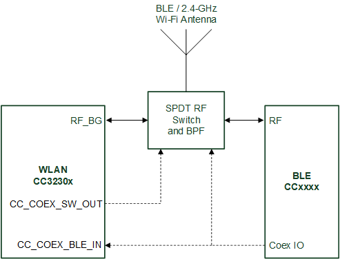
CC3230S CC3230SF Single-Antenna Coexistence Mode Block DiagramFigure 9-1 Single-Antenna Coexistence Mode Block Diagram


Figure 9-2 shows the dual antenna implementation of a complete Bluetooth low energy and WLAN coexistence network. Note in this implementation no Coex switch is required and only a single GPIO from the BLE device to the CC3230x device is required.
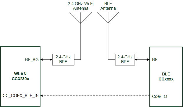
CC3230S CC3230SF Dual-Antenna Coexistence Mode Block DiagramFigure 9-2 Dual-Antenna Coexistence Mode Block Diagram