SWRS243C February 2020 – December 2024 CC3235MODAS , CC3235MODASF , CC3235MODS , CC3235MODSF
PRODUCTION DATA
- 1
- 1 Features
- 2 Applications
- 3 Description
- 4 Functional Block Diagrams
- 5 Device Comparison
- 6 Pin Configuration and Functions
-
7 Specifications
- 7.1 Absolute Maximum Ratings
- 7.2 ESD Ratings
- 7.3 Recommended Operating Conditions
- 7.4 Current Consumption (CC3235MODS and CC3235MODAS)
- 7.5 Current Consumption (CC3235MODSF and CC3235MODASF)
- 7.6 TX Power Control for 2.4 GHz Band
- 7.7 TX Power Control for 5 GHz
- 7.8 Brownout and Blackout Conditions
- 7.9 Electrical Characteristics for GPIO Pins
- 7.10 CC3235MODAx Antenna Characteristics
- 7.11 WLAN Receiver Characteristics
- 7.12 WLAN Transmitter Characteristics
- 7.13 BLE and WLAN Coexistence Requirements
- 7.14 Reset Requirement
- 7.15 Thermal Resistance Characteristics for MOB and MON Packages
- 7.16
Timing and Switching Characteristics
- 7.16.1 Power-Up Sequencing
- 7.16.2 Power-Down Sequencing
- 7.16.3 Device Reset
- 7.16.4 Wake Up From Hibernate Timing
- 7.16.5 Peripherals Timing
-
8 Detailed Description
- 8.1 Overview
- 8.2 Functional Block Diagram
- 8.3 Arm Cortex-M4 Processor Core Subsystem
- 8.4 Wi-Fi Network Processor Subsystem
- 8.5 Security
- 8.6 FIPS 140-2 Level 1 Certification
- 8.7 Power-Management Subsystem
- 8.8 Low-Power Operating Mode
- 8.9 Memory
- 8.10 Restoring Factory Default Configuration
- 8.11 Boot Modes
- 8.12 Hostless Mode
- 8.13 Device Certification and Qualification
- 8.14 Module Markings
- 8.15 End Product Labeling
- 8.16 Manual Information to the End User
- 9 Applications, Implementation, and Layout
- 10Environmental Requirements and SMT Specifications
- 11Device and Documentation Support
- 12Revision History
- 13Mechanical, Packaging, and Orderable Information
Package Options
Refer to the PDF data sheet for device specific package drawings
Mechanical Data (Package|Pins)
- MON|63
Thermal pad, mechanical data (Package|Pins)
Orderable Information
9.3.2 CC3235MODx RF Layout Recommendations
The RF section of this wireless module gets top priority in terms of layout. It is very important for the RF section to be laid out correctly to ensure optimum performance from the module. A poor layout can cause low-output power, EVM degradation, sensitivity degradation, and mask violations.
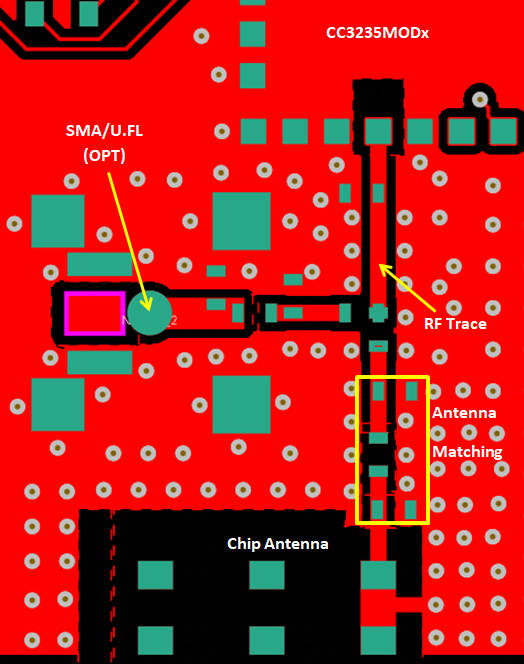
Figure 9-5 shows the RF placement and routing of the CC3235MODx module with external antenna.
 Figure 9-5 RF Section Layout
Follow these RF layout recommendations for the CC3235MODx device:
- RF traces must have 50Ω impedance.
- RF trace bends must be made with gradual curves, and 90° bends must be avoided.
- RF traces must not have sharp corners.
- There must be no traces or ground under the antenna section.
- RF traces must have via stitching on the ground plane beside the RF trace on both sides.
- RF traces must be as short as possible. The antenna, RF traces, and the module must be on the edge of the PCB product in consideration of the product enclosure material and proximity.
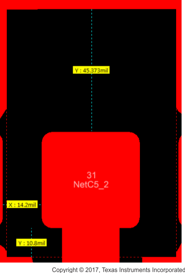
For optimal RF performance, ensure the copper cut out on the top layer under the RF-BG pin (pin 31) is as shown in Figure 9-6.
 Figure 9-6 Top Layer Copper Pullback on RF Pads