SWRS243C February   2020  – December 2024 CC3235MODAS , CC3235MODASF , CC3235MODS , CC3235MODSF

PRODUCTION DATA  

  1.   1
  2. Features
  3. Applications
  4. Description
  5. Functional Block Diagrams
  6. Device Comparison
    1. 5.1 Related Products
  7. Pin Configuration and Functions
    1. 6.1 CC3235MODx and CC3235MODAx Pin Diagram
    2. 6.2 Pin Attributes and Pin Multiplexing
      1. 6.2.1 Module Pin Descriptions
    3. 6.3 Signal Descriptions
    4. 6.4 Drive Strength and Reset States for Analog-Digital Multiplexed Pins
    5. 6.5 Pad State After Application of Power to Chip, but Before Reset Release
    6. 6.6 Connections for Unused Pins
  8. Specifications
    1. 7.1  Absolute Maximum Ratings
    2. 7.2  ESD Ratings
    3. 7.3  Recommended Operating Conditions
    4. 7.4  Current Consumption (CC3235MODS and CC3235MODAS)
      1.      21
      2.      22
    5. 7.5  Current Consumption (CC3235MODSF and CC3235MODASF)
      1.      24
      2.      25
    6. 7.6  TX Power Control for 2.4 GHz Band
    7. 7.7  TX Power Control for 5 GHz
    8. 7.8  Brownout and Blackout Conditions
    9. 7.9  Electrical Characteristics for GPIO Pins
      1. 7.9.1 Electrical Characteristics for Pin Internal Pullup and Pulldown (25°C)
    10. 7.10 CC3235MODAx Antenna Characteristics
    11. 7.11 WLAN Receiver Characteristics
      1.      33
      2.      34
    12. 7.12 WLAN Transmitter Characteristics
      1.      36
      2.      37
    13. 7.13 BLE and WLAN Coexistence Requirements
    14. 7.14 Reset Requirement
    15. 7.15 Thermal Resistance Characteristics for MOB and MON Packages
    16. 7.16 Timing and Switching Characteristics
      1. 7.16.1 Power-Up Sequencing
      2. 7.16.2 Power-Down Sequencing
      3. 7.16.3 Device Reset
      4. 7.16.4 Wake Up From Hibernate Timing
      5. 7.16.5 Peripherals Timing
        1. 7.16.5.1  SPI
          1. 7.16.5.1.1 SPI Master
          2. 7.16.5.1.2 SPI Slave
        2. 7.16.5.2  I2S
          1. 7.16.5.2.1 I2S Transmit Mode
          2. 7.16.5.2.2 I2S Receive Mode
        3. 7.16.5.3  GPIOs
          1. 7.16.5.3.1 GPIO Input Transition Time Parameters
        4. 7.16.5.4  I2C
        5. 7.16.5.5  IEEE 1149.1 JTAG
        6. 7.16.5.6  ADC
        7. 7.16.5.7  Camera Parallel Port
        8. 7.16.5.8  UART
        9. 7.16.5.9  External Flash Interface
        10. 7.16.5.10 SD Host
        11. 7.16.5.11 Timers
  9. Detailed Description
    1. 8.1  Overview
    2. 8.2  Functional Block Diagram
    3. 8.3  Arm Cortex-M4 Processor Core Subsystem
    4. 8.4  Wi-Fi Network Processor Subsystem
      1. 8.4.1 WLAN
      2. 8.4.2 Network Stack
    5. 8.5  Security
    6. 8.6  FIPS 140-2 Level 1 Certification
    7. 8.7  Power-Management Subsystem
      1. 8.7.1 VBAT Wide-Voltage Connection
    8. 8.8  Low-Power Operating Mode
    9. 8.9  Memory
      1. 8.9.1 Internal Memory
        1. 8.9.1.1 SRAM
        2. 8.9.1.2 ROM
        3. 8.9.1.3 Flash Memory
        4. 8.9.1.4 Memory Map
    10. 8.10 Restoring Factory Default Configuration
    11. 8.11 Boot Modes
      1. 8.11.1 Boot Mode List
    12. 8.12 Hostless Mode
    13. 8.13 Device Certification and Qualification
      1. 8.13.1 FCC Certification and Statement
      2. 8.13.2 IC/ISED Certification and Statement
      3. 8.13.3 ETSI/CE Certification
      4. 8.13.4 MIC Certification
    14. 8.14 Module Markings
    15. 8.15 End Product Labeling
    16. 8.16 Manual Information to the End User
  10. Applications, Implementation, and Layout
    1. 9.1 Typical Application
      1. 9.1.1 BLE/2.4GHz Radio Coexistence
      2. 9.1.2 Antenna Selection (CC3235MODx only)
      3. 9.1.3 Typical Application Schematic (CC3235MODx)
      4. 9.1.4 Typical Application Schematic (CC3235MODAx)
    2. 9.2 Device Connection and Layout Fundamentals
      1. 9.2.1 Power Supply Decoupling and Bulk Capacitors
      2. 9.2.2 Reset
      3. 9.2.3 Unused Pins
    3. 9.3 PCB Layout Guidelines
      1. 9.3.1 General Layout Recommendations
      2. 9.3.2 CC3235MODx RF Layout Recommendations
        1. 9.3.2.1 Antenna Placement and Routing
        2. 9.3.2.2 Transmission Line Considerations
      3. 9.3.3 CC3235MODAx RF Layout Recommendations
  11. 10Environmental Requirements and SMT Specifications
    1. 10.1 PCB Bending
    2. 10.2 Handling Environment
      1. 10.2.1 Terminals
      2. 10.2.2 Falling
    3. 10.3 Storage Condition
      1. 10.3.1 Moisture Barrier Bag Before Opened
      2. 10.3.2 Moisture Barrier Bag Open
    4. 10.4 PCB Assembly Guide
      1. 10.4.1 PCB Land Pattern and Thermal Vias
      2. 10.4.2 SMT Assembly Recommendations
      3. 10.4.3 PCB Surface Finish Requirements
      4. 10.4.4 Solder Stencil
      5. 10.4.5 Package Placement
      6. 10.4.6 Solder Joint Inspection
      7. 10.4.7 Rework and Replacement
      8. 10.4.8 Solder Joint Voiding
    5. 10.5 Baking Conditions
    6. 10.6 Soldering and Reflow Condition
  12. 11Device and Documentation Support
    1. 11.1 Development Tools and Software
    2. 11.2 Firmware Updates
    3. 11.3 Device Nomenclature
    4. 11.4 Documentation Support
    5. 11.5 Related Links
    6. 11.6 Support Resources
    7. 11.7 Trademarks
    8. 11.8 Electrostatic Discharge Caution
    9. 11.9 Glossary
  13. 12Revision History
  14. 13Mechanical, Packaging, and Orderable Information
    1. 13.1 Mechanical, Land, and Solder Paste Drawings
    2. 13.2 Package Option Addendum
      1. 13.2.1 Packaging Information
      2. 13.2.2 Tape and Reel Information
      3. 13.2.3 CC3235MODx Tape Specifications
      4. 13.2.4 CC3235MODAx Tape Specifications

Package Options

Refer to the PDF data sheet for device specific package drawings

Mechanical Data (Package|Pins)
  • MOB|63
Thermal pad, mechanical data (Package|Pins)
Orderable Information

Power-Up Sequencing

For proper start-up of the CC3235MODx and CC3235MODAx module, perform the recommended power-up sequencing as follows:

  1. Tie VBAT1 (pin 37) and VBAT2 (pin 40) together on the board.
  2. Hold the nRESET pin low while the supplies are ramping up.

Figure 7-6 shows the reset timing diagram for the first-time power-up and reset removal.
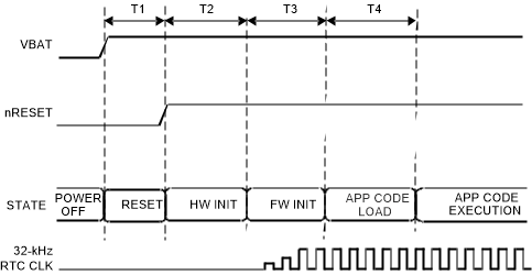
CC3235MODS CC3235MODSF CC3235MODAS CC3235MODASF First-Time Power-Up and Reset Removal Timing DiagramFigure 7-6 First-Time Power-Up and Reset Removal Timing Diagram


Table 7-13 lists the timing requirements for the first-time power-up and reset removal.

Table 7-13 First-Time Power-Up and Reset Removal Timing Requirements
ITEMNAMEDESCRIPTIONMINTYPMAXUNIT
T1nReset timenReset timing after VBAT supplies are stable1ms
T2Hardware wake-up time25ms
T3Time taken by ROM firmware to initialize hardwareIncludes internal 32kHz XOSC settling time1.1s
T4App code load time for CC3235MODS and CC3235MODASCC3235MODS and CC3235MODASImage size (KB) × 1.7 ms
App code load time for CC3235MODSF and CC3235MODASFCC3235MODSF and CC3235MODASFImage size (KB) × 0.06 ms