SWRS243C February 2020 – December 2024 CC3235MODAS , CC3235MODASF , CC3235MODS , CC3235MODSF
PRODUCTION DATA
- 1
- 1 Features
- 2 Applications
- 3 Description
- 4 Functional Block Diagrams
- 5 Device Comparison
- 6 Pin Configuration and Functions
-
7 Specifications
- 7.1 Absolute Maximum Ratings
- 7.2 ESD Ratings
- 7.3 Recommended Operating Conditions
- 7.4 Current Consumption (CC3235MODS and CC3235MODAS)
- 7.5 Current Consumption (CC3235MODSF and CC3235MODASF)
- 7.6 TX Power Control for 2.4 GHz Band
- 7.7 TX Power Control for 5 GHz
- 7.8 Brownout and Blackout Conditions
- 7.9 Electrical Characteristics for GPIO Pins
- 7.10 CC3235MODAx Antenna Characteristics
- 7.11 WLAN Receiver Characteristics
- 7.12 WLAN Transmitter Characteristics
- 7.13 BLE and WLAN Coexistence Requirements
- 7.14 Reset Requirement
- 7.15 Thermal Resistance Characteristics for MOB and MON Packages
- 7.16
Timing and Switching Characteristics
- 7.16.1 Power-Up Sequencing
- 7.16.2 Power-Down Sequencing
- 7.16.3 Device Reset
- 7.16.4 Wake Up From Hibernate Timing
- 7.16.5 Peripherals Timing
-
8 Detailed Description
- 8.1 Overview
- 8.2 Functional Block Diagram
- 8.3 Arm Cortex-M4 Processor Core Subsystem
- 8.4 Wi-Fi Network Processor Subsystem
- 8.5 Security
- 8.6 FIPS 140-2 Level 1 Certification
- 8.7 Power-Management Subsystem
- 8.8 Low-Power Operating Mode
- 8.9 Memory
- 8.10 Restoring Factory Default Configuration
- 8.11 Boot Modes
- 8.12 Hostless Mode
- 8.13 Device Certification and Qualification
- 8.14 Module Markings
- 8.15 End Product Labeling
- 8.16 Manual Information to the End User
- 9 Applications, Implementation, and Layout
- 10Environmental Requirements and SMT Specifications
- 11Device and Documentation Support
- 12Revision History
- 13Mechanical, Packaging, and Orderable Information
Package Options
Refer to the PDF data sheet for device specific package drawings
Mechanical Data (Package|Pins)
- MOB|63
Thermal pad, mechanical data (Package|Pins)
Orderable Information
9.3.2.2 Transmission Line Considerations
The RF signal from the module is routed to the antenna using a Coplanar Waveguide with ground (CPW-G) structure. CPW-G structure offers the maximum amount of isolation and the best possible shielding to the RF lines. In addition to the ground on the L1 layer, placing GND vias along the line also provides additional shielding.
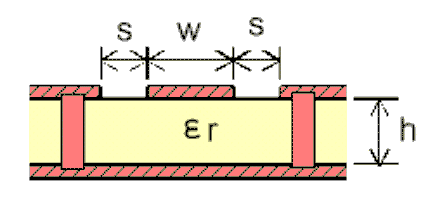
Figure 9-7 shows a cross section of the coplanar waveguide with the critical dimensions.
Figure 4-1 shows the top view of the coplanar waveguide with GND and via stitching.
 Figure 9-7 Coplanar Waveguide (Cross Section)
 Figure 9-8 CPW With GND and Via Stitching (Top View)
The recommended values for the PCB are provided for 2-layer boards in Table 9-5 and 4-layer boards in Table 9-6.
| PARAMETER | VALUE | UNIT |
|---|---|---|
| W | 26 | mils |
| S | 5.5 | mils |
| H | 42.1 | mils |
| Er (FR-4 substrate) | 4.2 | F/m |
| PARAMETER | VALUE | UNITS |
|---|---|---|
| W | 21 | mils |
| S | 10 | mils |
| H | 16 | mils |
| Er (FR-4 substrate) | 4.5 | F/m |