SWRS243C February   2020  – December 2024 CC3235MODAS , CC3235MODASF , CC3235MODS , CC3235MODSF

PRODUCTION DATA  

  1.   1
  2. Features
  3. Applications
  4. Description
  5. Functional Block Diagrams
  6. Device Comparison
    1. 5.1 Related Products
  7. Pin Configuration and Functions
    1. 6.1 CC3235MODx and CC3235MODAx Pin Diagram
    2. 6.2 Pin Attributes and Pin Multiplexing
      1. 6.2.1 Module Pin Descriptions
    3. 6.3 Signal Descriptions
    4. 6.4 Drive Strength and Reset States for Analog-Digital Multiplexed Pins
    5. 6.5 Pad State After Application of Power to Chip, but Before Reset Release
    6. 6.6 Connections for Unused Pins
  8. Specifications
    1. 7.1  Absolute Maximum Ratings
    2. 7.2  ESD Ratings
    3. 7.3  Recommended Operating Conditions
    4. 7.4  Current Consumption (CC3235MODS and CC3235MODAS)
      1.      21
      2.      22
    5. 7.5  Current Consumption (CC3235MODSF and CC3235MODASF)
      1.      24
      2.      25
    6. 7.6  TX Power Control for 2.4 GHz Band
    7. 7.7  TX Power Control for 5 GHz
    8. 7.8  Brownout and Blackout Conditions
    9. 7.9  Electrical Characteristics for GPIO Pins
      1. 7.9.1 Electrical Characteristics for Pin Internal Pullup and Pulldown (25°C)
    10. 7.10 CC3235MODAx Antenna Characteristics
    11. 7.11 WLAN Receiver Characteristics
      1.      33
      2.      34
    12. 7.12 WLAN Transmitter Characteristics
      1.      36
      2.      37
    13. 7.13 BLE and WLAN Coexistence Requirements
    14. 7.14 Reset Requirement
    15. 7.15 Thermal Resistance Characteristics for MOB and MON Packages
    16. 7.16 Timing and Switching Characteristics
      1. 7.16.1 Power-Up Sequencing
      2. 7.16.2 Power-Down Sequencing
      3. 7.16.3 Device Reset
      4. 7.16.4 Wake Up From Hibernate Timing
      5. 7.16.5 Peripherals Timing
        1. 7.16.5.1  SPI
          1. 7.16.5.1.1 SPI Master
          2. 7.16.5.1.2 SPI Slave
        2. 7.16.5.2  I2S
          1. 7.16.5.2.1 I2S Transmit Mode
          2. 7.16.5.2.2 I2S Receive Mode
        3. 7.16.5.3  GPIOs
          1. 7.16.5.3.1 GPIO Input Transition Time Parameters
        4. 7.16.5.4  I2C
        5. 7.16.5.5  IEEE 1149.1 JTAG
        6. 7.16.5.6  ADC
        7. 7.16.5.7  Camera Parallel Port
        8. 7.16.5.8  UART
        9. 7.16.5.9  External Flash Interface
        10. 7.16.5.10 SD Host
        11. 7.16.5.11 Timers
  9. Detailed Description
    1. 8.1  Overview
    2. 8.2  Functional Block Diagram
    3. 8.3  Arm Cortex-M4 Processor Core Subsystem
    4. 8.4  Wi-Fi Network Processor Subsystem
      1. 8.4.1 WLAN
      2. 8.4.2 Network Stack
    5. 8.5  Security
    6. 8.6  FIPS 140-2 Level 1 Certification
    7. 8.7  Power-Management Subsystem
      1. 8.7.1 VBAT Wide-Voltage Connection
    8. 8.8  Low-Power Operating Mode
    9. 8.9  Memory
      1. 8.9.1 Internal Memory
        1. 8.9.1.1 SRAM
        2. 8.9.1.2 ROM
        3. 8.9.1.3 Flash Memory
        4. 8.9.1.4 Memory Map
    10. 8.10 Restoring Factory Default Configuration
    11. 8.11 Boot Modes
      1. 8.11.1 Boot Mode List
    12. 8.12 Hostless Mode
    13. 8.13 Device Certification and Qualification
      1. 8.13.1 FCC Certification and Statement
      2. 8.13.2 IC/ISED Certification and Statement
      3. 8.13.3 ETSI/CE Certification
      4. 8.13.4 MIC Certification
    14. 8.14 Module Markings
    15. 8.15 End Product Labeling
    16. 8.16 Manual Information to the End User
  10. Applications, Implementation, and Layout
    1. 9.1 Typical Application
      1. 9.1.1 BLE/2.4GHz Radio Coexistence
      2. 9.1.2 Antenna Selection (CC3235MODx only)
      3. 9.1.3 Typical Application Schematic (CC3235MODx)
      4. 9.1.4 Typical Application Schematic (CC3235MODAx)
    2. 9.2 Device Connection and Layout Fundamentals
      1. 9.2.1 Power Supply Decoupling and Bulk Capacitors
      2. 9.2.2 Reset
      3. 9.2.3 Unused Pins
    3. 9.3 PCB Layout Guidelines
      1. 9.3.1 General Layout Recommendations
      2. 9.3.2 CC3235MODx RF Layout Recommendations
        1. 9.3.2.1 Antenna Placement and Routing
        2. 9.3.2.2 Transmission Line Considerations
      3. 9.3.3 CC3235MODAx RF Layout Recommendations
  11. 10Environmental Requirements and SMT Specifications
    1. 10.1 PCB Bending
    2. 10.2 Handling Environment
      1. 10.2.1 Terminals
      2. 10.2.2 Falling
    3. 10.3 Storage Condition
      1. 10.3.1 Moisture Barrier Bag Before Opened
      2. 10.3.2 Moisture Barrier Bag Open
    4. 10.4 PCB Assembly Guide
      1. 10.4.1 PCB Land Pattern and Thermal Vias
      2. 10.4.2 SMT Assembly Recommendations
      3. 10.4.3 PCB Surface Finish Requirements
      4. 10.4.4 Solder Stencil
      5. 10.4.5 Package Placement
      6. 10.4.6 Solder Joint Inspection
      7. 10.4.7 Rework and Replacement
      8. 10.4.8 Solder Joint Voiding
    5. 10.5 Baking Conditions
    6. 10.6 Soldering and Reflow Condition
  12. 11Device and Documentation Support
    1. 11.1 Development Tools and Software
    2. 11.2 Firmware Updates
    3. 11.3 Device Nomenclature
    4. 11.4 Documentation Support
    5. 11.5 Related Links
    6. 11.6 Support Resources
    7. 11.7 Trademarks
    8. 11.8 Electrostatic Discharge Caution
    9. 11.9 Glossary
  13. 12Revision History
  14. 13Mechanical, Packaging, and Orderable Information
    1. 13.1 Mechanical, Land, and Solder Paste Drawings
    2. 13.2 Package Option Addendum
      1. 13.2.1 Packaging Information
      2. 13.2.2 Tape and Reel Information
      3. 13.2.3 CC3235MODx Tape Specifications
      4. 13.2.4 CC3235MODAx Tape Specifications

Package Options

Refer to the PDF data sheet for device specific package drawings

Mechanical Data (Package|Pins)
  • MOB|63
Thermal pad, mechanical data (Package|Pins)
Orderable Information

TX Power Control for 2.4 GHz Band

The CC3235MODS and CC3235MODAS has several options for modifying the output power of the device when required. For the 2.4 GHz band it is possible to lower the overall output power at a global level using the global TX power level setting. In addition, the 2.4 GHz band allows the user to enter additional back-offs (2), per channel, region (3)and modulation rates (4)(5), through Image creator (see the Uniflash with Image Creator User Guide for more details).

Figure 7-1, Figure 7-2, and Figure 7-3 show TX power and IBAT versus TX power level settings for the CC3235MODS module at modulations of 1 DSSS, 6 OFDM, and 54 OFDM, respectively. For the CC3235MODSF module, the IBAT current has an increase of approximately 10 mA to 15 mA depending on the transmitted rate. The TX power level remains the same.4

In Figure 7-1, the area enclosed in the circle represents a significant reduction in current during transition from TX power level 3 to level 4. In the case of lower range requirements (14-dBm output power), TI recommends using TX power level 4 to reduce the current.
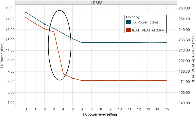
 

CC3235MODS CC3235MODSF CC3235MODAS CC3235MODASF TX Power and IBAT vs TX Power Level Settings (1 DSSS)Figure 7-1 TX Power and IBAT vs TX Power Level Settings (1 DSSS)
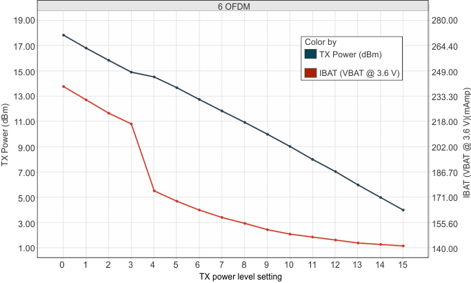
CC3235MODS CC3235MODSF CC3235MODAS CC3235MODASF TX Power and IBAT vs TX Power Level Settings (6 OFDM)Figure 7-2 TX Power and IBAT vs TX Power Level Settings (6 OFDM)
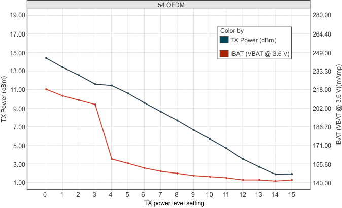


CC3235MODS CC3235MODSF CC3235MODAS CC3235MODASF TX Power and IBAT vs TX Power Level Settings (54 OFDM)Figure 7-3 TX Power and IBAT vs TX Power Level Settings (54 OFDM)
The back-off range is between –6 dB to +6 dB in 0.25-dB increments.
FCC, IC/ISED, ETSI/CE, MIC, and SRRC are supported.
Back-off rates are grouped into 11b rates, high modulation rates (MCS7, 54 OFDM and 48 OFDM), and lower modulation rates (all other rates).
There will be a difference between the CC3135MOD and CC3135 IC TX power levels.