SWRS215E April   2019  – December 2024 CC3235S , CC3235SF

PRODUCTION DATA  

  1.   1
  2. Features
  3. Applications
  4. Description
  5. Functional Block Diagrams
  6. Device Comparison
    1. 5.1 Related Products
  7. Pin Configuration and Functions
    1. 6.1 Pin Diagram
    2. 6.2 Pin Attributes
      1.      11
    3. 6.3 Signal Descriptions
      1.      13
    4. 6.4 Pin Multiplexing
    5. 6.5 Drive Strength and Reset States for Analog and Digital Multiplexed Pins
    6. 6.6 Pad State After Application of Power to Device, Before Reset Release
    7. 6.7 Connections for Unused Pins
  8. Specifications
    1. 7.1  Absolute Maximum Ratings
    2. 7.2  ESD Ratings
    3. 7.3  Power-On Hours (POH)
    4. 7.4  Recommended Operating Conditions
    5. 7.5  Current Consumption Summary (CC3235S)
      1.      24
      2.      25
    6. 7.6  Current Consumption Summary (CC3235SF)
      1.      27
      2.      28
    7. 7.7  TX Power Control for 2.4 GHz Band
    8. 7.8  TX Power Control for 5 GHz
    9. 7.9  Brownout and Blackout Conditions
    10. 7.10 Electrical Characteristics for GPIO Pins
      1.      33
      2.      34
    11. 7.11 Electrical Characteristics for Pin Internal Pullup and Pulldown
    12. 7.12 WLAN Receiver Characteristics
      1.      37
      2.      38
    13. 7.13 WLAN Transmitter Characteristics
      1.      40
      2.      41
    14. 7.14 WLAN Transmitter Out-of-Band Emissions
      1.      43
      2.      44
    15. 7.15 BLE/2.4 GHz Radio Coexistence and WLAN Coexistence Requirements
    16. 7.16 Thermal Resistance Characteristics for RGK Package
    17. 7.17 Timing and Switching Characteristics
      1. 7.17.1 Power Supply Sequencing
      2. 7.17.2 Device Reset
      3. 7.17.3 Reset Timing
        1. 7.17.3.1 nRESET (32kHz Crystal)
        2.       52
        3.       53
        4. 7.17.3.2 nRESET (External 32kHz Clock)
          1.        55
      4. 7.17.4 Wakeup From HIBERNATE Mode
      5. 7.17.5 Clock Specifications
        1. 7.17.5.1 Slow Clock Using Internal Oscillator
        2. 7.17.5.2 Slow Clock Using an External Clock
          1.        60
        3. 7.17.5.3 Fast Clock (Fref) Using an External Crystal
          1.        62
        4. 7.17.5.4 Fast Clock (Fref) Using an External Oscillator
          1.        64
      6. 7.17.6 Peripherals Timing
        1. 7.17.6.1  SPI
          1. 7.17.6.1.1 SPI Master
            1.         68
          2. 7.17.6.1.2 SPI Slave
            1.         70
        2. 7.17.6.2  I2S
          1. 7.17.6.2.1 I2S Transmit Mode
            1.         73
          2. 7.17.6.2.2 I2S Receive Mode
            1.         75
        3. 7.17.6.3  GPIOs
          1. 7.17.6.3.1 GPIO Output Transition Time Parameters (Vsupply = 3.3V)
            1.         78
          2. 7.17.6.3.2 GPIO Input Transition Time Parameters
            1.         80
        4. 7.17.6.4  I2C
          1.        82
        5. 7.17.6.5  IEEE 1149.1 JTAG
          1.        84
        6. 7.17.6.6  ADC
          1.        86
        7. 7.17.6.7  Camera Parallel Port
          1.        88
        8. 7.17.6.8  UART
        9. 7.17.6.9  SD Host
        10. 7.17.6.10 Timers
  9. Detailed Description
    1. 8.1  Overview
    2. 8.2  Arm® Cortex®-M4 Processor Core Subsystem
    3. 8.3  Wi-Fi® Network Processor Subsystem
      1. 8.3.1 WLAN
      2. 8.3.2 Network Stack
    4. 8.4  Security
    5. 8.5  FIPS 140-2 Level 1 Certification
    6. 8.6  Power-Management Subsystem
    7. 8.7  Low-Power Operating Mode
    8. 8.8  Memory
      1. 8.8.1 External Memory Requirements
      2. 8.8.2 Internal Memory
        1. 8.8.2.1 SRAM
        2. 8.8.2.2 ROM
        3. 8.8.2.3 Flash Memory
        4. 8.8.2.4 Memory Map
    9. 8.9  Restoring Factory Default Configuration
    10. 8.10 Boot Modes
      1. 8.10.1 Boot Mode List
    11. 8.11 Hostless Mode
  10. Applications, Implementation, and Layout
    1. 9.1 Application Information
      1. 9.1.1 BLE/2.4GHz Radio Coexistence
      2. 9.1.2 Antenna Selection
      3. 9.1.3 Typical Application
    2. 9.2 PCB Layout Guidelines
      1. 9.2.1 General PCB Guidelines
      2. 9.2.2 Power Layout and Routing
        1. 9.2.2.1 Design Considerations
      3. 9.2.3 Clock Interface Guidelines
      4. 9.2.4 Digital Input and Output Guidelines
      5. 9.2.5 RF Interface Guidelines
  11. 10Device and Documentation Support
    1. 10.1  Third-Party Products Disclaimer
    2. 10.2  Tools and Software
    3. 10.3  Firmware Updates
    4. 10.4  Device Nomenclature
    5. 10.5  Documentation Support
    6. 10.6  Related Links
    7. 10.7  Support Resources
    8. 10.8  Trademarks
    9. 10.9  Electrostatic Discharge Caution
    10. 10.10 Export Control Notice
    11. 10.11 Glossary
  12. 11Revision History
  13. 12Mechanical, Packaging, and Orderable Information
    1. 12.1 Packaging Information
      1. 12.1.1 Packaging Option Addendum

Package Options

Mechanical Data (Package|Pins)
Thermal pad, mechanical data (Package|Pins)
Orderable Information

Wakeup From HIBERNATE Mode

Note:

The 32.768kHz crystal is enabled by default when the chip goes into HIBERNATE mode.

Table 7-17 lists the software hibernate timing requirements.

Table 7-17 Software Hibernate Timing Requirements
ITEMNAMEDESCRIPTIONMINTYPMAXUNIT
THIB_MINMinimum hibernate time10ms
Twake_from_hib(1)Hardware wakeup time plus firmware initialization time50(2)ms
T_APP_CODE_LOADApp code load time for CC3235SCC3235SImage size (KB) × 1.7msms
App code load time for CC3235SFCC3235SFImage size (KB) × 0.06ms
Twake_from_hib can be 200ms on rare occasions when calibration is performed. Calibration is performed sparingly, typically when exiting Hibernate and only if temperature has changed by more than 20°C or more than 24 hours have elapsed since a prior calibration.
Wake-up time can extend to 75ms if a patch is downloaded from the serial Flash.


Figure 7-8 shows the timing diagram for wakeup from HIBERNATE mode.
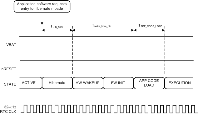
CC3235S CC3235SF Wakeup From HIBERNATE Timing DiagramFigure 7-8 Wakeup From HIBERNATE Timing Diagram