SWRS215D April   2019  – May 2021 CC3235S , CC3235SF

PRODUCTION DATA  

  1. Features
  2. Applications
  3. Description
  4. Functional Block Diagrams
  5. Revision History
  6. Device Comparison
    1. 6.1 Related Products
  7. Terminal Configuration and Functions
    1. 7.1 Pin Diagram
    2. 7.2 Pin Attributes
      1.      11
    3. 7.3 Signal Descriptions
      1.      13
    4. 7.4 Pin Multiplexing
    5. 7.5 Drive Strength and Reset States for Analog and Digital Multiplexed Pins
    6. 7.6 Pad State After Application of Power to Device, Before Reset Release
    7. 7.7 Connections for Unused Pins
  8. Specifications
    1. 8.1  Absolute Maximum Ratings
    2. 8.2  ESD Ratings
    3. 8.3  Power-On Hours (POH)
    4. 8.4  Recommended Operating Conditions
    5. 8.5  Current Consumption Summary (CC3235S)
      1.      24
      2.      25
    6. 8.6  Current Consumption Summary (CC3235SF)
      1.      27
      2.      28
    7. 8.7  TX Power Control for 2.4 GHz Band
    8. 8.8  TX Power Control for 5 GHz
    9. 8.9  Brownout and Blackout Conditions
    10. 8.10 Electrical Characteristics for GPIO Pins
      1.      33
      2.      34
    11. 8.11 Electrical Characteristics for Pin Internal Pullup and Pulldown
    12. 8.12 WLAN Receiver Characteristics
      1.      37
      2.      38
    13. 8.13 WLAN Transmitter Characteristics
      1.      40
      2.      41
    14. 8.14 WLAN Transmitter Out-of-Band Emissions
      1.      43
      2.      44
    15. 8.15 BLE/2.4 GHz Radio Coexistence and WLAN Coexistence Requirements
    16. 8.16 Thermal Resistance Characteristics for RGK Package
    17. 8.17 Timing and Switching Characteristics
      1. 8.17.1 Power Supply Sequencing
      2. 8.17.2 Device Reset
      3. 8.17.3 Reset Timing
        1. 8.17.3.1 nRESET (32-kHz Crystal)
        2.       52
        3.       53
        4. 8.17.3.2 nRESET (External 32-kHz Clock)
          1.        55
      4. 8.17.4 Wakeup From HIBERNATE Mode
      5. 8.17.5 Clock Specifications
        1. 8.17.5.1 Slow Clock Using Internal Oscillator
        2. 8.17.5.2 Slow Clock Using an External Clock
          1.        60
        3. 8.17.5.3 Fast Clock (Fref) Using an External Crystal
          1.        62
        4. 8.17.5.4 Fast Clock (Fref) Using an External Oscillator
          1.        64
      6. 8.17.6 Peripherals Timing
        1. 8.17.6.1  SPI
          1. 8.17.6.1.1 SPI Master
            1.         68
          2. 8.17.6.1.2 SPI Slave
            1.         70
        2. 8.17.6.2  I2S
          1. 8.17.6.2.1 I2S Transmit Mode
            1.         73
          2. 8.17.6.2.2 I2S Receive Mode
            1.         75
        3. 8.17.6.3  GPIOs
          1. 8.17.6.3.1 GPIO Output Transition Time Parameters (Vsupply = 3.3 V)
            1.         78
          2. 8.17.6.3.2 GPIO Input Transition Time Parameters
            1.         80
        4. 8.17.6.4  I2C
          1.        82
        5. 8.17.6.5  IEEE 1149.1 JTAG
          1.        84
        6. 8.17.6.6  ADC
          1.        86
        7. 8.17.6.7  Camera Parallel Port
          1.        88
        8. 8.17.6.8  UART
        9. 8.17.6.9  SD Host
        10. 8.17.6.10 Timers
  9. Detailed Description
    1. 9.1  Overview
    2. 9.2  Arm® Cortex®-M4 Processor Core Subsystem
    3. 9.3  Wi-Fi® Network Processor Subsystem
      1. 9.3.1 WLAN
      2. 9.3.2 Network Stack
    4. 9.4  Security
    5. 9.5  FIPS 140-2 Level 1 Certification
    6. 9.6  Power-Management Subsystem
    7. 9.7  Low-Power Operating Mode
    8. 9.8  Memory
      1. 9.8.1 External Memory Requirements
      2. 9.8.2 Internal Memory
        1. 9.8.2.1 SRAM
        2. 9.8.2.2 ROM
        3. 9.8.2.3 Flash Memory
        4. 9.8.2.4 Memory Map
    9. 9.9  Restoring Factory Default Configuration
    10. 9.10 Boot Modes
      1. 9.10.1 Boot Mode List
    11. 9.11 Hostless Mode
  10. 10Applications, Implementation, and Layout
    1. 10.1 Application Information
      1. 10.1.1 BLE/2.4 GHz Radio Coexistence
      2. 10.1.2 Antenna Selection
      3. 10.1.3 Typical Application
    2. 10.2 PCB Layout Guidelines
      1. 10.2.1 General PCB Guidelines
      2. 10.2.2 Power Layout and Routing
        1. 10.2.2.1 Design Considerations
      3. 10.2.3 Clock Interface Guidelines
      4. 10.2.4 Digital Input and Output Guidelines
      5. 10.2.5 RF Interface Guidelines
  11. 11Device and Documentation Support
    1. 11.1  Third-Party Products Disclaimer
    2. 11.2  Tools and Software
    3. 11.3  Firmware Updates
    4. 11.4  Device Nomenclature
    5. 11.5  Documentation Support
    6. 11.6  Related Links
    7. 11.7  Support Resources
    8. 11.8  Trademarks
    9. 11.9  Electrostatic Discharge Caution
    10. 11.10 Export Control Notice
    11. 11.11 Glossary
  12. 12Mechanical, Packaging, and Orderable Information
    1. 12.1 Packaging Information
      1. 12.1.1 Package Option Addendum
        1. 12.1.1.1 Packaging Information
        2. 12.1.1.2 Tape and Reel Information

Package Options

Mechanical Data (Package|Pins)
Thermal pad, mechanical data (Package|Pins)
Orderable Information

Slow Clock Using Internal Oscillator

The RTC crystal connected on the device supplies the free-running slow clock. The accuracy of the slow clock frequency must be 32.768 kHz ±150 ppm. In this mode of operation, the crystal is tied between RTC_XTAL_P (pin 51) and RTC_XTAL_N (pin 52) with a suitable load capacitance to meet the ppm requirement.

Figure 8-9 shows the crystal connections for the slow clock.
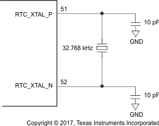
GUID-71884258-9BEC-48E6-8570-2782BF290408-low.gifFigure 8-9 RTC Crystal Connections


Table 8-18 lists the RTC crystal requirements.

Table 8-18 RTC Crystal Requirements
CHARACTERISTICSTEST CONDITIONSMINTYPMAXUNIT
Frequency32.768kHz
Frequency accuracyInitial plus temperature plus aging±150ppm
Crystal ESR32.768 kHz70