SWRS215D April   2019  – May 2021 CC3235S , CC3235SF

PRODUCTION DATA  

  1. Features
  2. Applications
  3. Description
  4. Functional Block Diagrams
  5. Revision History
  6. Device Comparison
    1. 6.1 Related Products
  7. Terminal Configuration and Functions
    1. 7.1 Pin Diagram
    2. 7.2 Pin Attributes
      1.      11
    3. 7.3 Signal Descriptions
      1.      13
    4. 7.4 Pin Multiplexing
    5. 7.5 Drive Strength and Reset States for Analog and Digital Multiplexed Pins
    6. 7.6 Pad State After Application of Power to Device, Before Reset Release
    7. 7.7 Connections for Unused Pins
  8. Specifications
    1. 8.1  Absolute Maximum Ratings
    2. 8.2  ESD Ratings
    3. 8.3  Power-On Hours (POH)
    4. 8.4  Recommended Operating Conditions
    5. 8.5  Current Consumption Summary (CC3235S)
      1.      24
      2.      25
    6. 8.6  Current Consumption Summary (CC3235SF)
      1.      27
      2.      28
    7. 8.7  TX Power Control for 2.4 GHz Band
    8. 8.8  TX Power Control for 5 GHz
    9. 8.9  Brownout and Blackout Conditions
    10. 8.10 Electrical Characteristics for GPIO Pins
      1.      33
      2.      34
    11. 8.11 Electrical Characteristics for Pin Internal Pullup and Pulldown
    12. 8.12 WLAN Receiver Characteristics
      1.      37
      2.      38
    13. 8.13 WLAN Transmitter Characteristics
      1.      40
      2.      41
    14. 8.14 WLAN Transmitter Out-of-Band Emissions
      1.      43
      2.      44
    15. 8.15 BLE/2.4 GHz Radio Coexistence and WLAN Coexistence Requirements
    16. 8.16 Thermal Resistance Characteristics for RGK Package
    17. 8.17 Timing and Switching Characteristics
      1. 8.17.1 Power Supply Sequencing
      2. 8.17.2 Device Reset
      3. 8.17.3 Reset Timing
        1. 8.17.3.1 nRESET (32-kHz Crystal)
        2.       52
        3.       53
        4. 8.17.3.2 nRESET (External 32-kHz Clock)
          1.        55
      4. 8.17.4 Wakeup From HIBERNATE Mode
      5. 8.17.5 Clock Specifications
        1. 8.17.5.1 Slow Clock Using Internal Oscillator
        2. 8.17.5.2 Slow Clock Using an External Clock
          1.        60
        3. 8.17.5.3 Fast Clock (Fref) Using an External Crystal
          1.        62
        4. 8.17.5.4 Fast Clock (Fref) Using an External Oscillator
          1.        64
      6. 8.17.6 Peripherals Timing
        1. 8.17.6.1  SPI
          1. 8.17.6.1.1 SPI Master
            1.         68
          2. 8.17.6.1.2 SPI Slave
            1.         70
        2. 8.17.6.2  I2S
          1. 8.17.6.2.1 I2S Transmit Mode
            1.         73
          2. 8.17.6.2.2 I2S Receive Mode
            1.         75
        3. 8.17.6.3  GPIOs
          1. 8.17.6.3.1 GPIO Output Transition Time Parameters (Vsupply = 3.3 V)
            1.         78
          2. 8.17.6.3.2 GPIO Input Transition Time Parameters
            1.         80
        4. 8.17.6.4  I2C
          1.        82
        5. 8.17.6.5  IEEE 1149.1 JTAG
          1.        84
        6. 8.17.6.6  ADC
          1.        86
        7. 8.17.6.7  Camera Parallel Port
          1.        88
        8. 8.17.6.8  UART
        9. 8.17.6.9  SD Host
        10. 8.17.6.10 Timers
  9. Detailed Description
    1. 9.1  Overview
    2. 9.2  Arm® Cortex®-M4 Processor Core Subsystem
    3. 9.3  Wi-Fi® Network Processor Subsystem
      1. 9.3.1 WLAN
      2. 9.3.2 Network Stack
    4. 9.4  Security
    5. 9.5  FIPS 140-2 Level 1 Certification
    6. 9.6  Power-Management Subsystem
    7. 9.7  Low-Power Operating Mode
    8. 9.8  Memory
      1. 9.8.1 External Memory Requirements
      2. 9.8.2 Internal Memory
        1. 9.8.2.1 SRAM
        2. 9.8.2.2 ROM
        3. 9.8.2.3 Flash Memory
        4. 9.8.2.4 Memory Map
    9. 9.9  Restoring Factory Default Configuration
    10. 9.10 Boot Modes
      1. 9.10.1 Boot Mode List
    11. 9.11 Hostless Mode
  10. 10Applications, Implementation, and Layout
    1. 10.1 Application Information
      1. 10.1.1 BLE/2.4 GHz Radio Coexistence
      2. 10.1.2 Antenna Selection
      3. 10.1.3 Typical Application
    2. 10.2 PCB Layout Guidelines
      1. 10.2.1 General PCB Guidelines
      2. 10.2.2 Power Layout and Routing
        1. 10.2.2.1 Design Considerations
      3. 10.2.3 Clock Interface Guidelines
      4. 10.2.4 Digital Input and Output Guidelines
      5. 10.2.5 RF Interface Guidelines
  11. 11Device and Documentation Support
    1. 11.1  Third-Party Products Disclaimer
    2. 11.2  Tools and Software
    3. 11.3  Firmware Updates
    4. 11.4  Device Nomenclature
    5. 11.5  Documentation Support
    6. 11.6  Related Links
    7. 11.7  Support Resources
    8. 11.8  Trademarks
    9. 11.9  Electrostatic Discharge Caution
    10. 11.10 Export Control Notice
    11. 11.11 Glossary
  12. 12Mechanical, Packaging, and Orderable Information
    1. 12.1 Packaging Information
      1. 12.1.1 Package Option Addendum
        1. 12.1.1.1 Packaging Information
        2. 12.1.1.2 Tape and Reel Information

Package Options

Mechanical Data (Package|Pins)
Thermal pad, mechanical data (Package|Pins)
Orderable Information

TX Power Control for 2.4 GHz Band

The CC3235x has several options for modifying the output power of the device when required. For the 2.4 GHz band it is possible to lower the overall output power at a global level using the global TX power level setting. In addition, the 2.4 GHz band allows the user to enter additional back-offs (2), per channel, region (3)and modulation rates (4), via Image creator (see the Uniflash with Image Creator User Guide for more details).

Figure 8-1, Figure 8-2, and Figure 8-3 show TX power and IBAT versus TX power level settings for the CC3235S device at modulations of 1 DSSS, 6 OFDM, and 54 OFDM, respectively. For the CC3235SF device, the IBAT current has an increase of approximately 10 mA to 15 mA depending on the transmitted rate. The TX power level will remain the same.

In Figure 8-1, the area enclosed in the circle represents a significant reduction in current during transition from TX power level 3 to level 4. In the case of lower range requirements (14-dBm output power), TI recommends using TX power level 4 to reduce the current.

GUID-0230D56F-A13D-4412-9BE2-9F195B779F71-low.gifFigure 8-1 TX Power and IBAT vs TX Power Level Settings (1 DSSS)


GUID-0CEB5A6E-C13C-4469-97FB-E4ED21B608B6-low.gifFigure 8-2 TX Power and IBAT vs TX Power Level Settings (6 OFDM)
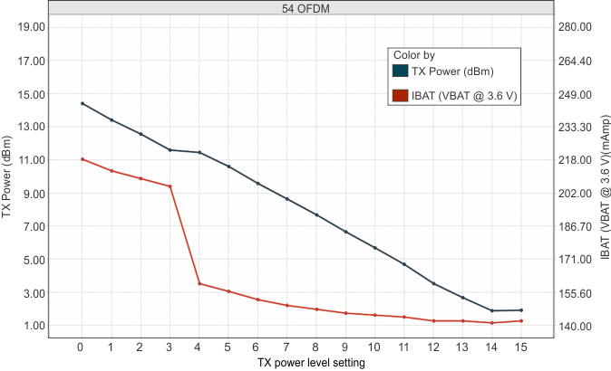
GUID-6CAA94A3-A024-46E1-BD21-DDA823B9B121-low.gifFigure 8-3 TX Power and IBAT vs TX Power Level Settings (54 OFDM)


The back-off range is between -6 dB to +6 dB in 0.25dB increments.
FCC/ISED, ETSI (Europe), and Japan are supported.
Back-off rates are grouped into 11b rates, high modulation rates (MCS7, 54 OFDM and 48 OFDM), and lower modulation rates (all other rates).