SCHS023E November 1998 – September 2016 CD4013B
PRODUCTION DATA.
- 1 Features
- 2 Applications
- 3 Description
- 4 Revision History
- 5 Pin Configuration and Functions
- 6 Specifications
- 7 Detailed Description
- 8 Application and Implementation
- 9 Power Supply Recommendations
- 10Layout
- 11Device and Documentation Support
- 12Mechanical, Packaging, and Orderable Information
Package Options
Refer to the PDF data sheet for device specific package drawings
Mechanical Data (Package|Pins)
- J|14
Thermal pad, mechanical data (Package|Pins)
Orderable Information
7 Detailed Description
7.1 Overview
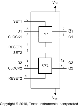
The CD4013B device consists of two identical, independent data-type flip-flops. Each flip-flop has independent data, set, reset, and clock inputs and Q and Q outputs. These devices are ideal for data and memory hold functions, including shift register applications, or by connecting Q output to the data input, this device is used for counter and toggle applications. The CD4013B is a positive-edge triggered device, meaning that the logic level present at the D input is transferred to the Q output during the positive-going transition of the clock pulse. Setting or resetting is independent of the clock and is accomplished by a high level on the set or reset line, respectively.
7.2 Functional Block Diagram

7.3 Feature Description
CD4013B has standardized symmetrical output characteristics and a wide operating voltage range from 3 V to
18 V with quiescent current tested at 20 V. This has a medium operation speed –tPHL, tPLH = 30 ns (typical) at 10 V. The operating temperature is from –55°C to 125°C.
7.4 Device Functional Modes
Table 1 lists the functional modes of the CD4013B.
Table 1. Function Table
| INPUTS | OUTPUT (Q) | INVERTED OUTPUT (Q) | |||
|---|---|---|---|---|---|
| CLOCK | SET | RESET | D | ||
| ↑ | 0 | 0 | 0 | 0 | 1 |
| ↑ | 0 | 0 | 1 | 1 | 0 |
| ↓ | 0 | 0 | X | Q0 | Q |
| X | 0 | 1 | X | 0 | 1 |
| X | 1 | 0 | X | 1 | 0 |
| X | 1 | 1 | X | 1 | 1 |