SCHS023E November 1998 – September 2016 CD4013B
PRODUCTION DATA.
- 1 Features
- 2 Applications
- 3 Description
- 4 Revision History
- 5 Pin Configuration and Functions
- 6 Specifications
- 7 Detailed Description
- 8 Application and Implementation
- 9 Power Supply Recommendations
- 10Layout
- 11Device and Documentation Support
- 12Mechanical, Packaging, and Orderable Information
Package Options
Refer to the PDF data sheet for device specific package drawings
Mechanical Data (Package|Pins)
- D|14
- PW|14
- N|14
- NS|14
Thermal pad, mechanical data (Package|Pins)
Orderable Information
10 Layout
10.1 Layout Guidelines
When using multiple bit logic devices, inputs must never float.
In many cases, digital logic device functions or parts of these functions are unused (for example, when only two inputs of a triple-input and gate are used, or only 3 of the 4 buffer gates are used). Such input pins must not be left unconnected because the undefined voltages at the outside connections result in undefined operational states. This rule must be observed under all circumstances specified in the next paragraph.
All unused inputs of digital logic devices must be connected to a high or low bias to prevent them from floating. See application note, Implications of Slow or Floating CMOS Inputs (SCBA004), for more information on the effects of floating inputs. The logic level must apply to any particular unused input depending on the function of the device. Generally, they are tied to GND or VCC (whichever is convenient).
10.2 Layout Example
 Figure 11. Layout Example for CD4013B
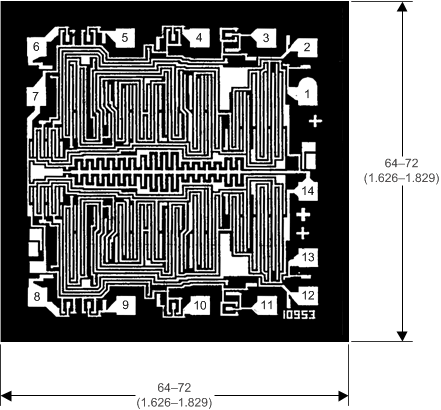
 Figure 12. Dimensions and Pad Layout for CD4013B