SCHS026E November 1998 – August 2024 CD4016B
PRODUCTION DATA
- 1
- 1Features
- 2Applications
- 3Description
- 4Specifications
- 5Parameter Measurement Information
- 6Device and Documentation Support
- 7Revision History
- 8Mechanical, Packaging, and Orderable Information
Package Options
Refer to the PDF data sheet for device specific package drawings
Mechanical Data (Package|Pins)
- J|14
Thermal pad, mechanical data (Package|Pins)
Orderable Information
5 Parameter Measurement Information
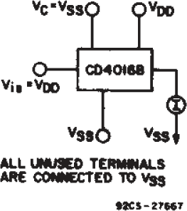 Figure 5-1 Off-state Switch Input or
Output Leakage Current Test Circuit.
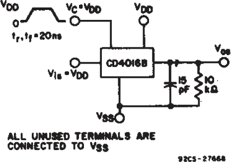 Figure 5-2 Test Circuit for
Square-wave Response.
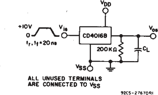 Figure 5-3 Propagation Delay Time
Signal Input (vIS) To Signal Output (vOS)
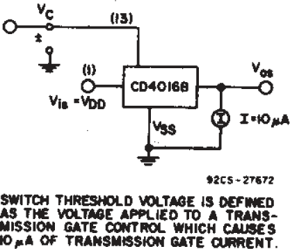 Figure 5-5 Switch Threshold
Voltage.
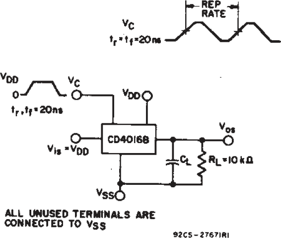 Figure 5-4 MAX Control-input
Repetition Rate.
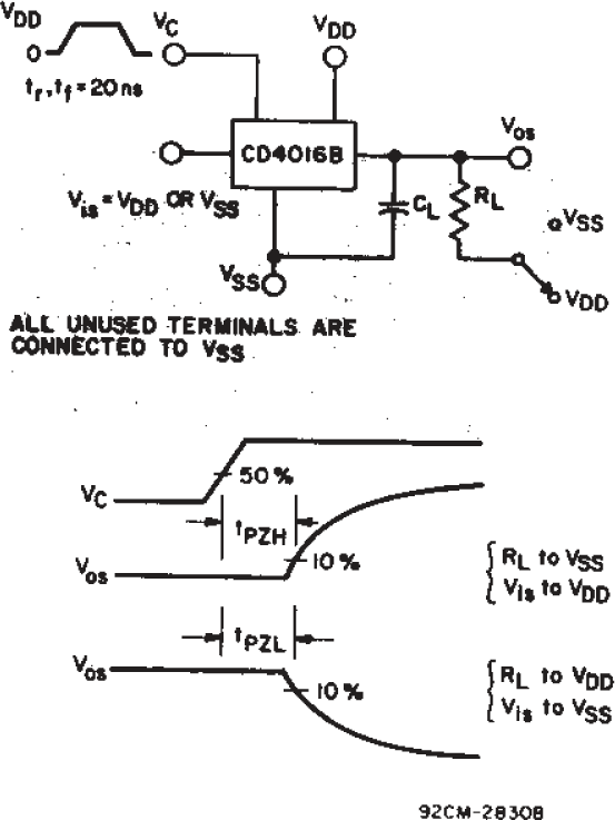 Figure 5-6 Turn-On Propagation
Delay-control Input.