SCHS026D November 1998 – May 2024 CD4016B
PRODUCTION DATA
- 1
- 1Features
- 2Applications
- 3Description
- 4Specifications
- 5Parameter Measurement Information
- 6Device and Documentation Support
- 7Revision History
- 8Mechanical, Packaging, and Orderable Information
Package Options
Refer to the PDF data sheet for device specific package drawings
Mechanical Data (Package|Pins)
- D|14
- PW|14
- N|14
- NS|14
Thermal pad, mechanical data (Package|Pins)
Orderable Information
3 Description
For transmission or multiplexing of analog or digital signals high-voltage types (20V rating).
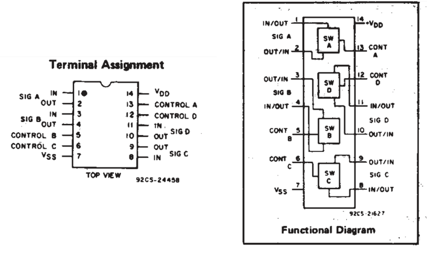
CD4016B B Series types are quad bilateral switches intended for the transmission or multiplexing of analog or digital signals. Each of the four independent bilateral switches has a single control signal input which simultaneously biases both the p and n device in a given switch on or off.
The CD4016B B Series types are supplied in 14-lead hermetic dual-in-line ceramic packages (F3A suffix), 14-lead dual-in-line plastic packages (E suffix), 14-lead small-outline packages (M, MT, M96, and NSR suffixes), and 14-lead thin shrink small-outline packages (PW and PWR suffixes).
| PART NUMBER | PACKAGE(1) | PACKAGE SIZE(2) |
|---|---|---|
| CD4016B | N (PDIP, 14) | 19.3mm × 9.4mm |
| D (SOIC, 14) | 8.65mm × 6mm |
 Schematic Diagram - 1 of 4 Identical Sections