SCHS051J November 1998 – August 2024 CD4066B
PRODUCTION DATA
- 1
- 1 Features
- 2 Applications
- 3 Description
- 4 Pin Configuration and Functions
- 5 Specifications
- 6 Parameter Measurement Information
- 7 Detailed Description
- 8 Application and Implementation
- 9 Device and Documentation Support
- 10Revision History
- 11Mechanical, Packaging, and Orderable Information
Package Options
Refer to the PDF data sheet for device specific package drawings
Mechanical Data (Package|Pins)
- D|14
- PW|14
- N|14
- NS|14
Thermal pad, mechanical data (Package|Pins)
Orderable Information
3 Description
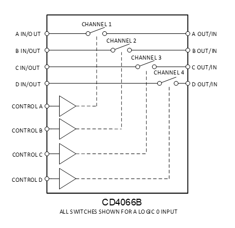
The CD4066B device is a quad bilateral switch intended for the transmission or multiplexing of analog or digital signals. It is pin-for-pin compatible with the CD4016B device, but exhibits a much lower on-state resistance. In addition, the on-state resistance is relatively constant over the full signal-input range.
The CD4066B device consists of four bilateral switches, each with independent controls. Wide operating supply of 3V to 18V allows for use in a broad array of applications. The advantages over single-channel switches include peak input-signal voltage swings equal to the full supply voltage and more constant on-state impedance over the input-signal range. However, for sample-and-hold applications, the CD4016B device is recommended.
| PART NUMBER | PACKAGE(1) | PACKAGE SIZE(2) |
|---|---|---|
| CD4066B | N (PDIP, 14) | 19.3mm × 9.4mm |
| D (SOIC, 14) | 8.65mm × 6mm | |
| NS (SOP, 14) | 10.2mm × 7.8mm | |
| PW (TSSOP, 14) | 5mm × 6.4mm |
 Bidirectional Signal Transmission Through Digital Control Logic