SCHS052D June 2003 – August 2024 CD4067B , CD4097B
PRODUCTION DATA
- 1
- 1 Features
- 2 Applications
- 3 Description
- 4 Pin Configuration and Functions
- 5 Specifications
- 6 Parameter Measurement Information
- 7 Detailed Description
- 8 Application and Implementation
- 9 Device and Documentation Support
- 10Revision History
- 11Mechanical, Packaging, and Orderable Information
Package Options
Refer to the PDF data sheet for device specific package drawings
Mechanical Data (Package|Pins)
- J|24
Thermal pad, mechanical data (Package|Pins)
Orderable Information
3 Description
CD40x7B CMOS analog multiplexers or demultiplexers are digitally controlled analog switches having low ON impedance, low OFF leakage current, and internal address decoding. When these devices are used as demultiplexers, the channel in or out terminals are the outputs and the common out or in terminals are the inputs. In addition, the ON resistance is relatively constant over the full input-signal range.
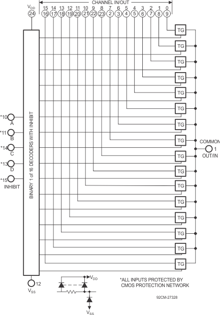
The CD4067B is a 16-channel multiplexer with four binary control inputs, A, B, C, D, and an inhibit input, arranged so that any combination of the inputs selects one switch.
A logic "1" present at the inhibit input turns all channels off.
The CD40x7B types are supplied in 24-lead hermetic dual-in-line ceramic packages (F3A suffix), 24-lead dual-in-line plastic packages (E suffix), 24-lead small-outline packages (M, M96, and NSR suffixes), and 24-lead thin shrink small-outline packages (P and PWR suffixes).
| PART NUMBER | CHANNEL | PACKAGE (1) |
|---|---|---|
| CD4067B | 2 channel 8:1 differential multiplexer | PW (TSSOP, 24) |
| DW (SOIC, 24) |
 CD4067 Logic Diagram
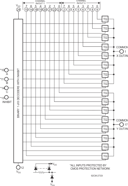
 CD4097 Logic Diagram