SCHS239D November 1998 – May 2024 CD54AC161 , CD74AC161
PRODUCTION DATA
- 1
- 1 Features
- 2 Description
- 3 Pin Configuration and Functions
- 4 Specifications
- 5 Parameter Measurement Information
- 6 Detailed Description
- 7 Application and Implementation
- 8 Device and Documentation Support
- 9 Revision History
- 10Mechanical, Packaging, and Orderable Information
Package Options
Refer to the PDF data sheet for device specific package drawings
Mechanical Data (Package|Pins)
- J|16
Thermal pad, mechanical data (Package|Pins)
Orderable Information
3 Pin Configuration and Functions
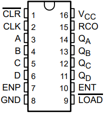
 Figure 3-1 CD54AC161 F Package, CD74AC161
E or M Package (Top View)
Figure 3-1 CD54AC161 F Package, CD74AC161
E or M Package (Top View)| NAME | PIN | TYPE | DESCRIPTION |
|---|---|---|---|
| CLR | 1 | I | Clear, active low |
| CLK | 2 | I | Clock, rising edge triggered |
| A | 3 | I | Load data A |
| B | 4 | I | Load data B |
| C | 5 | I | Load data C |
| D | 6 | I | Load data D |
| ENP | 7 | I | Count enable, does not affect RCO |
| GND | 8 | — | Ground |
| LOAD | 9 | I | Parallel load, active low |
| ENT | 10 | I | Count enable, affects RCO |
| QD | 11 | O | QD output |
| QC | 12 | O | QC output |
| QB | 13 | O | QB output |
| QA | 14 | O | QA output |
| RCO | 15 | O | Ripple-carry output |
| VCC | 16 | __ | Supply |