SCHS240D November   1998  – October 2024 CD54AC164 , CD54ACT164 , CD74AC164 , CD74ACT164

PRODUCTION DATA  

  1.   1
  2. Features
  3. Description
  4. Pin Configuration and Functions
  5. Specifications
    1. 4.1 Absolute Maximum Ratings
    2. 4.2 ESD Ratings
    3. 4.3 Recommended Operating Conditions
    4. 4.4 Thermal Information
    5. 4.5 DC Electrical Specifications
    6. 4.6 Prerequisite for Switching Function
    7. 4.7 Switching Specifications
  6. Parameter Measurement Information
  7. Detailed Description
    1. 6.1 Overview
    2. 6.2 Functional Block Diagram
    3. 6.3 Feature Description
      1. 6.3.1 Standard CMOS Inputs
      2. 6.3.2 TTL-Compatible CMOS Inputs
    4. 6.4 Device Functional Modes
  8. Application and Implementation
    1. 7.1 Application Information
    2. 7.2 Typical Application
      1. 7.2.1 Design Requirements
        1. 7.2.1.1 Power Considerations
        2. 7.2.1.2 Input Considerations
        3. 7.2.1.3 Output Considerations
        4. 7.2.1.4 Application Curve
    3. 7.3 Power Supply Recommendations
    4. 7.4 Layout
      1. 7.4.1 Layout Guidelines
      2. 7.4.2 Layout Example
  9. Device and Documentation Support
    1. 8.1 Documentation Support
      1. 8.1.1 Related Documentation
    2. 8.2 Receiving Notification of Documentation Updates
    3. 8.3 Support Resources
    4. 8.4 Trademarks
    5. 8.5 Electrostatic Discharge Caution
    6. 8.6 Glossary
  10. Device and Documentation Support
    1. 9.1 Documentation Support (Analog)
      1. 9.1.1 Related Documentation
    2. 9.2 Receiving Notification of Documentation Updates
    3. 9.3 Support Resources
    4. 9.4 Trademarks
    5. 9.5 Electrostatic Discharge Caution
    6. 9.6 Glossary
  11. 10Revision History
  12. 11Mechanical, Packaging, and Orderable Information

Refer to the PDF data sheet for device specific package drawings

Mechanical Data (Package|Pins)
  • J|14
Thermal pad, mechanical data (Package|Pins)

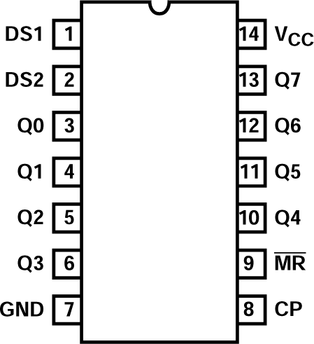
Pin Configuration and Functions

CD54AC164 CD74AC164 CD54ACT164 CD74ACT164 CD54AC(T)164 J Package;
                        14-Pin CDIP; CD74AC(T)164 D, N, or PW Package; 14-Pin SOIC, PDIP, or TSSOP
                        (Top View)Figure 3-1 CD54AC(T)164 J Package; 14-Pin CDIP; CD74AC(T)164 D, N, or PW Package; 14-Pin SOIC, PDIP, or TSSOP (Top View)
CD54AC164 CD74AC164 CD54ACT164 CD74ACT164 CD74AC(T)164 BQA Package;
                        14-Pin WQFN (Top View)Figure 3-2 CD74AC(T)164 BQA Package; 14-Pin WQFN (Top View)
Table 3-1 Pin Functions
PIN TYPE1 DESCRIPTION
NAME NO.
A 1 I Gated serial input A
B 2 I Gated serial input B
QA 3 O Parallel output A
QB 4 O Parallel output B
QC 5 O Parallel output C
QD 6 O Parallel output D
GND 7 G Ground
CLK 8 I Clock input, rising edge triggered
CLR 9 I Asynchronous register clear input, active low
QE 10 O Parallel output E
QF 11 O Parallel output F
QG 12 O Parallel output G
QH 13 O Parallel output H
VCC 14 P Positive supply
Thermal pad2 The thermal pad can be connect to GND or left floating. Do not connect to any other signal or supply.
  1. Signal Types: I = Input, O = Output, P = Power, G = Ground.
  2. BQA package only.