SCHS273F August   1997  – April 2021 CD54HC11 , CD74HC11

PRODUCTION DATA  

  1. Features
  2. Applications
  3. Description
  4. Revision History
    1.     5
      1.      Pin Functions
  5. Specifications
    1. 5.1 Absolute Maximum Ratings
    2. 5.2 ESD Ratings
    3. 5.3 Recommended Operating Conditions
    4. 5.4 Thermal Information
    5. 5.5 Electrical Characteristics
    6. 5.6 Switching Characteristics
    7. 5.7 Operating Characteristics
    8. 5.8 Typical Characteristics
  6. Parameter Measurement Information
  7. Detailed Description
    1. 7.1 Overview
    2. 7.2 Functional Block Diagram
    3. 7.3 Feature Description
      1. 7.3.1 Balanced CMOS Push-Pull Outputs
      2. 7.3.2 Standard CMOS Inputs
      3. 7.3.3 Clamp Diode Structure
    4. 7.4 Device Functional Modes
  8. Application and Implementation
    1. 8.1 Application Information
    2. 8.2 Typical Application
      1. 8.2.1 Design Requirements
        1. 8.2.1.1 Power Considerations
        2. 8.2.1.2 Input Considerations
        3. 8.2.1.3 Output Considerations
      2. 8.2.2 Detailed Design Procedure
      3. 8.2.3 Application Curves
  9. Layout
    1. 9.1 Layout Guidelines
    2. 9.2 Layout Example
  10. 10Device and Documentation Support
    1. 10.1 Documentation Support
      1. 10.1.1 Related Documentation
    2. 10.2 Receiving Notification of Documentation Updates
    3. 10.3 Support Resources
    4. 10.4 Trademarks
    5. 10.5 Electrostatic Discharge Caution
    6. 10.6 Related Links
    7. 10.7 Community Resources
    8. 10.8 Glossary

Package Options

Refer to the PDF data sheet for device specific package drawings

Mechanical Data (Package|Pins)
  • J|14
Thermal pad, mechanical data (Package|Pins)
Orderable Information

Description

This device contains three independent 3-input AND gates. Each gate performs the Boolean function Y = A ● B ● C in positive logic.

Device Information(1)
PART NUMBERPACKAGEBODY SIZE (NOM)
CD74HC11MSOIC (14)8.70 mm × 3.90 mm
CD74HC11EPDIP (14)19.30 mm × 6.40 mm
CD54HC11FCDIP (14)21.30 mm × 7.60 mm
For all available packages, see the orderable addendum at the end of the data sheet.
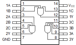
GUID-20722692-56B6-48B9-92B8-98CA067EA146-low.gif Functional pinout