SCHS173D November 1997 – November 2021 CD54HC259 , CD54HCT259 , CD74HC259 , CD74HCT259
PRODUCTION DATA
- 1 Features
- 2 Description
- 3 Revision History
- 4 Pin Configuration and Functions
- 5 Specifications
- 6 Parameter Measurement Information
- 7 Detailed Description
- 8 Power Supply Recommendations
- 9 Layout
- 10Device and Documentation Support
- 11Mechanical, Packaging, and Orderable Information
Package Options
Refer to the PDF data sheet for device specific package drawings
Mechanical Data (Package|Pins)
- J|16
Thermal pad, mechanical data (Package|Pins)
Orderable Information
2 Description
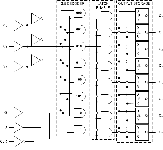
The CDx4HC(T)259 is an 8-bit addressable latch with three active modes of operation (addressable latch, memory, 8-line demultiplexer) and one reset mode.
Device Information
| PART NUMBER | PACKAGE(1) | BODY SIZE (NOM) |
|---|---|---|
| CD54HC259F3A | CDIP (16) | 21.34 mm × 6.92 mm |
| CD54HCT259F3A | CDIP (16) | 21.34 mm × 6.92 mm |
| CD74HC259E | PDIP (16) | 19.31 mm × 6.35 mm |
| CD74HCT259E | PDIP (16) | 19.31 mm × 6.35 mm |
| CD74HC259M | SOIC (16) | 9.90 mm × 3.90 mm |
| CD74HCT259M | SOIC (16) | 9.90 mm × 3.90 mm |
(1) For all packages see the
orderable addendum at the end of the data sheet.
 Functional Block
Diagram