SCHS181E November 1997 – February 2022 CD54HC367 , CD54HC368 , CD54HCT367 , CD74HC367 , CD74HC368 , CD74HCT367 , CD74HCT368
PRODUCTION DATA
- 1 Features
- 2 Description
- 3 Revision History
- 4 Pin Configuration and Functions
- 5 Specifications
- 6 Parameter Measurement Information
- 7 Detailed Description
- 8 Power Supply Recommendations
- 9 Layout
- 10Device and Documentation Support
- 11Mechanical, Packaging, and Orderable Information
Package Options
Refer to the PDF data sheet for device specific package drawings
Mechanical Data (Package|Pins)
- J|16
Thermal pad, mechanical data (Package|Pins)
Orderable Information
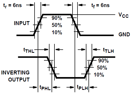
6 Parameter Measurement Information
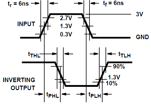
tpd is the maximum between tPLH and tPHL
tt is the maximum between tTLH and tTHL
 Figure 6-1 HC Transition Times and
Propagation Delay Times, Combination Logic
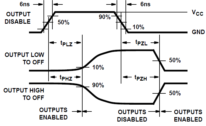
 Figure 6-3 HC Three-State Propagation
Delay Waveform
Note: Open drain waveforms
tPLZ and tPZL are the same as those for
three-state shown on the left. The test circuit is Output RL = 1
kΩ to VCC, CL = 50 pF.
Figure 6-5 HC and HCT Three-State
Propagation Delay Test Circuit Figure 6-2 HCT Transition Times and
Propagation Delay Times, Combination Logic
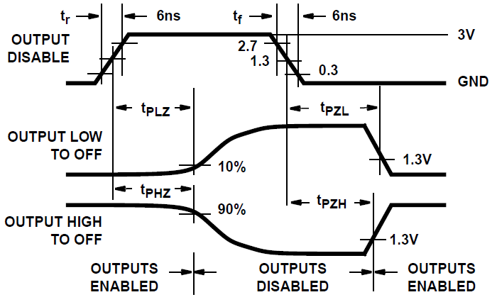
 Figure 6-4 HCT Three-State
Propagation Delay Waveform