SCHS122N November 1997 – April 2024 CD54HC4051 , CD54HC4052 , CD54HC4053 , CD54HCT4051 , CD74HC4051 , CD74HC4052 , CD74HC4053 , CD74HCT4051 , CD74HCT4052 , CD74HCT4053
PRODUCTION DATA
- 1
- 1 Features
- 2 Applications
- 3 Description
- 4 Pin Configuration and Functions
-
5 Specifications
- 5.1 Absolute Maximum Ratings
- 5.2 ESD Ratings
- 5.3 Thermal Information
- 5.4 Recommended Operating Conditions
- 5.5 Electrical Characteristics: HC Devices
- 5.6 Electrical Characteristics: HCT Devices
- 5.7 Switching Characteristics, VCC = 5V
- 5.8 Switching Characteristics, CL = 50pF
- 5.9 Analog Channel Specifications
- 5.10 Typical Characteristics
- 6 Parameter Measurement Information
- 7 Detailed Description
- 8 Application and Implementation
- 9 Device and Documentation Support
- 10Revision History
- 11Mechanical, Packaging, and Orderable Information
Package Options
Refer to the PDF data sheet for device specific package drawings
Mechanical Data (Package|Pins)
- J|16
Thermal pad, mechanical data (Package|Pins)
Orderable Information
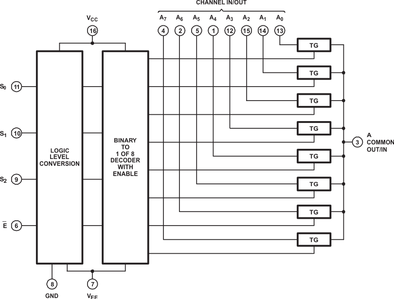
7.2 Functional Block Diagrams

All inputs are protected by standard CMOS protection network.
Figure 7-1 CDx4HCx4051 Functional Block Diagram
All inputs are protected by standard CMOS protection network.
Figure 7-2 CDx4HCx4052 Functional Block Diagram
All inputs are protected by standard CMOS protection network.
Figure 7-3 CDx4HCx4053 Functional Block Diagram