SCHS189E January 1998 – October 2022 CD54HC540 , CD54HC541 , CD54HCT541 , CD74HC540 , CD74HC541 , CD74HCT540 , CD74HCT541
PRODUCTION DATA
- 1 Features
- 2 Description
- 3 Revision History
- 4 Pin Configuration and Functions
- 5 Specifications
- 6 Parameter Measurement Information
- 7 Detailed Description
- 8 Power Supply Recommendations
- 9 Layout
- 10Device and Documentation Support
- 11Mechanical, Packaging, and Orderable Information
Package Options
Refer to the PDF data sheet for device specific package drawings
Mechanical Data (Package|Pins)
- J|20
Thermal pad, mechanical data (Package|Pins)
Orderable Information
2 Description
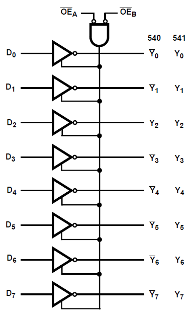
The ’HC540 and CD74HCT540 are Inverting Octal Buffers and Line Drivers with Three-State Outputs and the capability to drive 15 LSTTL loads. The ’HC541 and ’HCT541 are Noninverting Octal Buffers and Line Drivers with Three-State Outputs that can drive 15 LSTTL loads. The Output Enables (OE1) and (OE2) control the Three-State Outputs. If either OE1 or OE2 is HIGH the outputs will be in the high impedance state. For data output OE1 and OE2 both must be LOW.
| PART NUMBER | PACKAGE(1) | BODY SIZE (NOM) |
|---|---|---|
| CD74HC540M | SOIC (20) | 12.80 mm × 7.50 mm |
| CD74HC540E | PDIP (20) | 25.40 mm × 6.35 mm |
| CD54HC540F3A | CDIP (20) | 26.92 mm × 6.92 mm |
| CD74HC541M | SOIC (20) | 12.80 mm × 7.50 mm |
| CD74HC541E | PDIP (20) | 25.40 mm × 6.35 mm |
| CD54HC541F | CDIP (20) | 26.92 mm × 6.92 mm |
| CD74HCT540M | SOIC (20) | 12.80 mm × 7.50 mm |
| CD74HCT540E | PDIP (20) | 25.40 mm × 6.35 mm |
| CD74HCT541M | SOIC (20) | 12.80 mm × 7.50 mm |
| CD74HCT541E | PDIP (20) | 25.40 mm × 6.35 mm |
| CD54HCT541F | CDIP (20) | 26.92 mm × 6.92 mm |
| CD74HCT541PW | TSSOP (20) | 6.50 mm × 4.40 mm |
 Functional Diagram