SCHS141J March 1998 – October 2022 CD54HC112 , CD54HCT112 , CD74HC112 , CD74HCT112
PRODMIX
- 1 Features
- 2 Description
- 3 Revision History
- 4 Pin Configuration and Functions
- 5 Specifications
- 6 Parameter Measurement Information
- 7 Detailed Description
- 8 Power Supply Recommendations
- 9 Layout
- 10Device and Documentation Support
- 11Mechanical, Packaging, and Orderable Information
Package Options
Refer to the PDF data sheet for device specific package drawings
Mechanical Data (Package|Pins)
- J|16
Thermal pad, mechanical data (Package|Pins)
Orderable Information
2 Description
The ’HC112 and ’HCT112 utilize silicon-gate CMOS technology to achieve operating speeds equivalent to LSTTL parts. They exhibit the low power consumption of standard CMOS integrated circuits, together with the ability to drive 10 LSTTL loads.
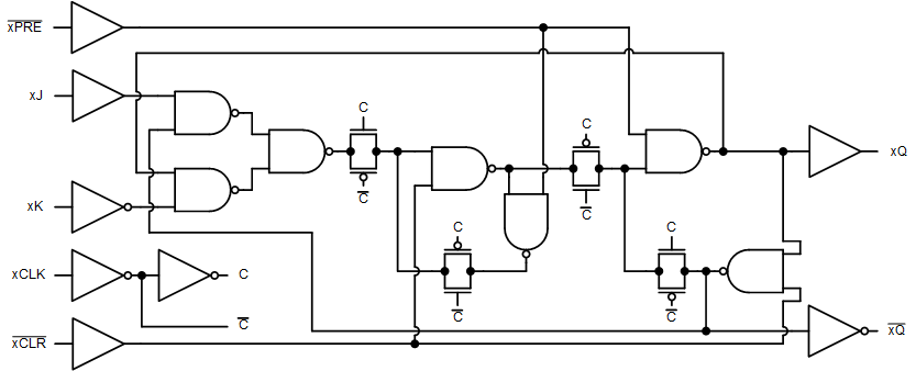
These flip-flops have independent J, K, PRE, CLR, and Clock inputs and Q and Q outputs. They change state on the negative-going transition of the clock pulse. PRE and CLR are accomplished asynchronously by low-level inputs.
The HCT logic family is functionally as well as pin compatible with the standard LS logic family.
| PART NUMBER | PACKAGE(1) | BODY SIZE (NOM) |
|---|---|---|
| CD54HC112F3A | CDIP (16) | 24.38 mm × 6.92 mm |
| CD74HC112M96 | SOIC (16) | 9.90 mm × 3.90 mm |
| CD74HC112E | PDIP (16) | 19.31 mm × 6.35 mm |
| CD74HCT112E | PDIP (16) | 19.31 mm × 6.35 mm |
| CD74HC112NSR | SO (16) | 6.20 mm × 5.30 mm |
| CD74HC112PW | TSSOP (16) | 5.00 mm × 4.40 mm |
 Functional
Diagram