SCHS415A June 2020 – August 2024 CD54HCT125 , CD74HCT125
PRODUCTION DATA
- 1
- 1 Features
- 2 Applications
- 3 Description
- 4 Pin Configuration and Functions
- 5 Specifications
- 6 Parameter Measurement Information
- 7 Detailed Description
- 8 Application and Implementation
- 9 Device and Documentation Support
- 10Revision History
- 11Mechanical, Packaging, and Orderable Information
Package Options
Mechanical Data (Package|Pins)
- J|14
Thermal pad, mechanical data (Package|Pins)
Orderable Information
3 Description
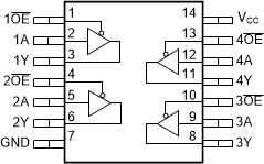
This device contains four independent buffers with 3-state outputs. Each gate performs the Boolean function Y = A in positive logic.
Device Information
| PART NUMBER | PACKAGE(1) | PACKAGE SIZE(2) | BODY SIZE(3) |
|---|---|---|---|
| CDx4HCT125 | D (SOIC, 14) | 8.65mm × 6mm | 8.65mm × 3.9mm |
| N (PDIP, 14) | 19.30mm × 9.4mm | 19.30mm × 6.35mm | |
| J (CDIP, 14) | 19.56mm x 6.7mm | 19.56mm × 4.57mm |
(1) For more information, see Mechanical, Packaging, and Orderable
Information.
(2) The package size (length × width) is a nominal value and includes pins, where
applicable.
(3) The body size (length × width) is a nominal value and does not include
pins.
 Functional pinout