SCLS453E February 2001 – June 2022 CD54HCT373 , CD74HCT373
PRODUCTION DATA
- 1 Features
- 2 Description
- 3 Revision History
- 4 Pin Configuration and Functions
- 5 Specifications
- 6 Parameter Measurement Information
- 7 Detailed Description
- 8 Power Supply Recommendations
- 9 Layout
- 10Device and Documentation Support
- 11Mechanical, Packaging, and Orderable Information
Package Options
Mechanical Data (Package|Pins)
- J|20
Thermal pad, mechanical data (Package|Pins)
Orderable Information
2 Description
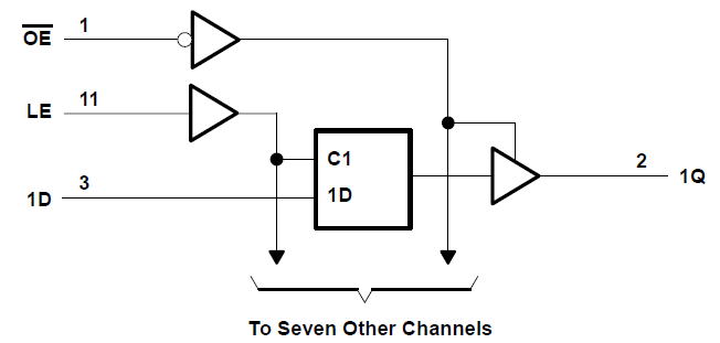
The ’HCT373 devices are octal transparent D-type latches. When the latch-enable (LE) input is high, the Q outputs follow the data (D) inputs. When LE is low, the Q outputs are latched at the logic levels of the D inputs.
Device
Information
| PART NUMBER | PACKAGE(1) | BODY SIZE (NOM) |
|---|---|---|
| CD74HCT373M | SOIC (20) | 12.80 mm × 7.50 mm |
| CD74HCT373E | PDIP (20) | 25.40 mm × 6.35 mm |
| CD54HCT373F | CDIP (20) | 26.92 mm × 6.92 mm |
(1) For all
available packages, see the orderable addendum at
the end of the data sheet.
 Funtional Block
Diagram