SCHS305E January 2001 – August 2024 CD54AC04 , CD74AC04
PRODUCTION DATA
- 1
- 1 Features
- 2 Description
- 3 Pin Configuration and Functions
-
4 Specifications
- 4.1 Absolute Maximum Ratings
- 4.2 ESD Ratings
- 4.3 Recommended Operating Conditions
- 4.4 Thermal Information
- 4.5 Electrical Characteristics
- 4.6 Switching Characteristics, VCC = 1.5 V
- 4.7 Switching Characteristics, VCC = 3.3 V ± 0.3 V
- 4.8 Switching Characteristics, VCC = 5 V ± 0.5 V
- 4.9 Operating Characteristics
- 5 Parameter Measurement Information
- 6 Detailed Description
- 7 Application and Implementation
- 8 Device and Documentation Support
- 9 Revision History
- 10Mechanical, Packaging, and Orderable Information
Package Options
Refer to the PDF data sheet for device specific package drawings
Mechanical Data (Package|Pins)
- D|14
- N|14
Thermal pad, mechanical data (Package|Pins)
Orderable Information
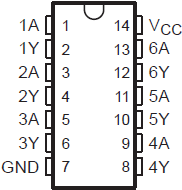
3 Pin Configuration and Functions
 Figure 3-1 CD54AC04 J Package, 14-Pin
CDIP; CD74AC04 N or D Package, 14-Pin SOIC or PDIP (Top View)
Figure 3-1 CD54AC04 J Package, 14-Pin
CDIP; CD74AC04 N or D Package, 14-Pin SOIC or PDIP (Top View)Table 3-1 Pin Functions
| PIN | I/O | DESCRIPTION | |
|---|---|---|---|
| NAME | NO. | ||
| 1A | 1 | Input | Channel 1, Input A |
| 1Y | 2 | Output | Channel 1, Output Y |
| 2A | 3 | Input | Channel 2, Input A |
| 2Y | 4 | Output | Channel 2, Output Y |
| 3A | 5 | Input | Channel 3, Input A |
| 3Y | 6 | Output | Channel 3, Output Y |
| GND | 7 | — | Ground |
| 4Y | 8 | Output | Channel 4, Output Y |
| 4A | 9 | Input | Channel 4, Input A |
| 5Y | 10 | Output | Channel 5, Output Y |
| 5A | 11 | Input | Channel 5, Input A |
| 6Y | 12 | Output | Channel 6, Output Y |
| 6A | 13 | Input | Channel 6, Input A |
| VCC | 14 | — | Positive Supply |