SCHS306E January 2001 – November 2024 CD54AC05 , CD74AC05
PRODUCTION DATA
- 1
- 1 Features
- 2 Description
- 3 Pin Configuration and Functions
-
4 Specifications
- 4.1 Absolute Maximum Ratings
- 4.2 ESD Ratings
- 4.3 Recommended Operating Conditions
- 4.4 Thermal Information
- 4.5 Electrical Characteristics
- 4.6 Switching Characteristics, VCC = 1.5 V
- 4.7 Switching Characteristics, VCC = 3.3 V ± 0.3 V
- 4.8 Switching Characteristics, VCC = 5 V ± 0.5 V
- 4.9 Operating Characteristics
- 5 Parameter Measurement Information
- 6 Detailed Description
- 7 Application and Implementation
- 8 Device and Documentation Support
- 9 Revision History
- 10Mechanical, Packaging, and Orderable Information
Package Options
Refer to the PDF data sheet for device specific package drawings
Mechanical Data (Package|Pins)
- D|14
- PW|14
- BQA|14
- N|14
Thermal pad, mechanical data (Package|Pins)
Orderable Information
3 Pin Configuration and Functions
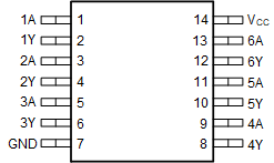
 Figure 3-1 CD54AC05 J Package, 14-Pin CDIP; CD74AC05 D, N, or PW Packages; 14-Pin SOIC, PDIP , or TSSOP (Top
View)
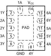
 Figure 3-2 CD74AC05 BQA Package, 14-Pin WQFN
Table 3-1 Pin Functions
| PIN | I/O(1) | DESCRIPTION | |||
|---|---|---|---|---|---|
| NAME | CD74AC05 | CD54AC05 | |||
| BQA, D, N, PW | J | ||||
| 1A | 1 | 1 | I | 1A Input | |
| 1Y | 2 | 2 | O | 1Y Output | |
| 2A | 3 | 3 | I | 2A Input | |
| 2Y | 4 | 4 | O | 2Y Output | |
| 3A | 5 | 5 | I | 3A Input | |
| 3Y | 6 | 6 | O | 3Y Output | |
| GND | 7 | 7 | — | Ground Pin | |
| 4Y | 8 | 8 | O | 4Y Output | |
| 4A | 9 | 9 | I | 4A Input | |
| 5Y | 10 | 10 | I | 5Y Output | |
| 5A | 11 | 11 | I | 5A Input | |
| 6Y | 12 | 12 | O | 6Y Output | |
| 6A | 13 | 13 | I | 6A Input | |
| VCC | 14 | 14 | — | Power Pin | |
| NC | — | — | — | No Connection | |
| Thermal pad | — | Connect the GND pin to the exposed thermal pad for correct operation. Connect the thermal pad to any internal PCB ground plane using multiple vias for good thermal performance. | |||
(1) I = input, O = output, P = power,
FB = feedback, GND = ground, N/A = not applicable