SCHS239D November 1998 – May 2024 CD54AC161 , CD74AC161
PRODUCTION DATA
- 1
- 1 Features
- 2 Description
- 3 Pin Configuration and Functions
- 4 Specifications
- 5 Parameter Measurement Information
- 6 Detailed Description
- 7 Application and Implementation
- 8 Device and Documentation Support
- 9 Revision History
- 10Mechanical, Packaging, and Orderable Information
Package Options
Refer to the PDF data sheet for device specific package drawings
Mechanical Data (Package|Pins)
- N|16
- D|16
Thermal pad, mechanical data (Package|Pins)
Orderable Information
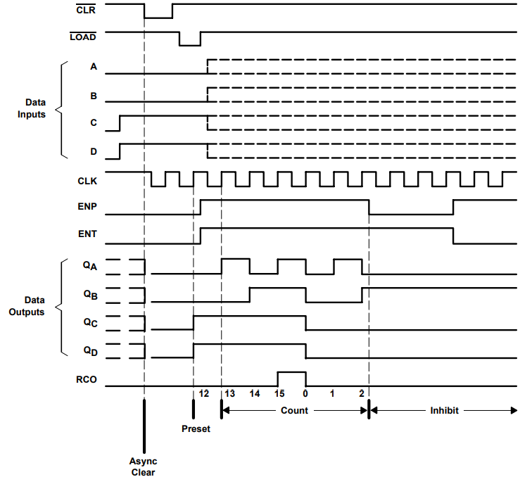
4.8 Timing Diagrams
The following sequence is illustrated below:
- Clear outputs to zero (asynchronous)
- Preset to binary 12
- Count to 13, 14, 15, 0, 1, and 2
- Inhibit
 Figure 4-1 Typical clear, preset, count, and inhibit sequence