SCHS239D November 1998 – May 2024 CD54AC161 , CD74AC161
PRODUCTION DATA
- 1
- 1 Features
- 2 Description
- 3 Pin Configuration and Functions
- 4 Specifications
- 5 Parameter Measurement Information
- 6 Detailed Description
- 7 Application and Implementation
- 8 Device and Documentation Support
- 9 Revision History
- 10Mechanical, Packaging, and Orderable Information
Package Options
Refer to the PDF data sheet for device specific package drawings
Mechanical Data (Package|Pins)
- N|16
- D|16
Thermal pad, mechanical data (Package|Pins)
- D|16
Orderable Information
2 Description
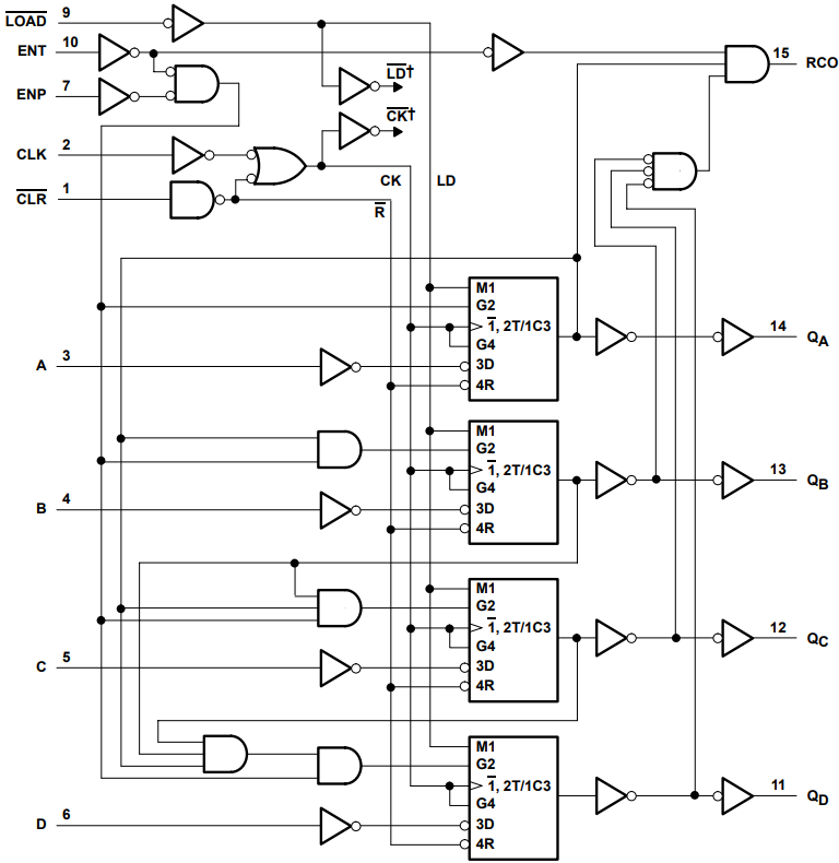
The ’AC161 devices are 4-bit binary counters. These synchronous, presettable counters feature an internal carry look-ahead for application in high-speed counting.
Device Information
| PART NUMBER | PACKAGE(1) | PACKAGE SIZE(2) | BODY SIZE(3) |
|---|---|---|---|
| CDx4AC161 | E (PDIP, 16) | 19.3mm x 9.4mm | 19.3mm x 6.35mm |
| M (SOIC, 16) | 9.9mm x 6mm | 9.9mm x 3.9mm |
(1) For all available packages, see the package option addendum at
the end of the data sheet.
(2) The package size (length × width) is a nominal value and includes pins, where
applicable.
(3) The body size (length × width) is
a nominal value and does not include pins.
 Logic Diagram (Positive Logic)